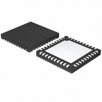
ISL6260CRZ Intersil, ISL6260CRZ Datasheet - Page 22

ISL6260CRZ
Manufacturer Part Number
ISL6260CRZ
Description
IC CORE REG MULTIPHASE 40-QFN
Manufacturer
Intersil
Datasheet
1.ISL6260BCRZ.pdf
(26 pages)
Specifications of ISL6260CRZ
Applications
Converter, Intel IMVP-6
Number Of Outputs
1
Voltage - Output
0.3 ~ 1.5 V
Operating Temperature
-10°C ~ 100°C
Mounting Type
Surface Mount
Package / Case
40-VFQFN, 40-VFQFPN
Lead Free Status / RoHS Status
Lead free / RoHS Compliant
Voltage - Input
-
Available stocks
Company
Part Number
Manufacturer
Quantity
Price
Company:
Part Number:
ISL6260CRZ
Manufacturer:
Intersil
Quantity:
74
Part Number:
ISL6260CRZ
Manufacturer:
INTERSIL
Quantity:
20 000
Part Number:
ISL6260CRZ-T
Manufacturer:
INTERSIL
Quantity:
20 000
We do this using the assumption that we desire
approximately a 0.57 gain from the DCR voltage, Vdcr, to the
Rn network. We call this gain, G1.
After simplification, then RS
equation:
The individual resistors from each phase to the VSUM node,
labeled RS1, RS2 and RS3 in Figure 42, are then given by
Equation 9, where N is 3, for the number of channels in
active operation.
Choosing RS = 7.68k_1% is a good choice. Once we know
the attenuation of the RS and RN network, we can then
determine the Droop amplifier Gain required to achieve the
load line. Setting Rdrp1 = 1k_1%, then Rdrp2 is can be
found using Equation 10.
Setting N = 3 for 3 channel operation, Droop Impedance
(Rdroop) = 0.0021 (V/A) as per the Intel IMVP-6
specification, DCR = 0.0012Ω typical, Rdrp1 = 1kΩ and the
attenuation gain (G1) = 0.57, Rdrp2 is then
Rdrp2
G1
RS
Rdrp2
RS
EQV
=
=
0.57
N
=
=
×
=
⎛
⎝
⎛
⎝
RS
N
------------------------------- - 1
----------------------------------- - 1
0.0012
⎛
⎝
DCR
------- - 1
G1
3
×
1
EQV
×
Rdroop
OC
–
0.0021
×
×
⎞ Rn
⎠
G1
=
Internal to
VDIFF
0.57
ISL6260
7.69kΩ
–
FIGURE 43. EQUIVALENT MODEL FOR DROOP AND DIE SENSING USING DCR SENSING
=
Σ
–
-
⎞
⎠
+
2.56kΩ
×
⎞
⎠
+
+
Rdrp1
×
EQV
10uA
22
1K
1
1
RTN
is given by the following
=
+
+
-
-
8.21kΩ
DROOP
VSEN
-
+
DROOP
OCSET
VSUM
DFB
ISL6260, ISL6260B
VO'
(EQ. 11)
(EQ. 10)
(EQ. 7)
(EQ. 8)
(EQ. 9)
Rdrp2 is selected to be a 8.25k_1% resistor. Note, we
choose to ignore the RO resistors because they do not add
significant error.
These values are extremely sensitive to layout and coupling
factor of the NTC to the inductor. As only one NTC is
required in this application, this NTC should be placed as
close to the Channel 1 inductor as possible and PCB traces
sensing the inductor voltage should be go directly to the
inductor pads.
Once the board has been laid out, some adjustments may
be required to adjust the full load droop voltage. This is fairly
easy and can be accomplished by allowing the system to
achieve thermal equilibrium at full load, and then adjusting
Rdrp2 to obtain the appropriate load line slope.
To see whether the NTC has compensated the temperature
change of the DCR, the user can apply full load current and
wait for the thermal steady state and see how much the
output voltage will deviate from the initial voltage reading. A
good compensation can limit the drift to 2mV. If the output
voltage is decreasing with temperature increase, that ratio
between the NTC thermistor value and the rest of the
resistor divider network has to be increased. The user
should follow the component values and layout of NTC on
evaluation board as much as possible to minimize
engineering time.
The 2.1mV/A load line should be adjusted by Rdrp2 based on
maximum current steps, not based on small current steps like
10A, as the droop gain might vary slightly between each 10A
steps. Basically, if the max current is 40A, the required droop
voltage is 84mV. The user should have 40A load current on
the converter and look for 84mV droop. If the droop voltage is
VSUM
VN
VO'
+
-
Rn
RS
=
EQV
RO
(
(
Rntc
Rntc
Vdcr
EQV
=
+
+
RS
EQV
N
Rseries
Rseries
=
RO
N
=
Iout
)
)
×
+
Rpar
Rpar
×
DCR
N
January 3, 2006
FN9162.1


