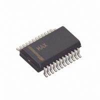
MAX8650EEG+ Maxim Integrated Products, MAX8650EEG+ Datasheet - Page 19

MAX8650EEG+
Manufacturer Part Number
MAX8650EEG+
Description
IC CNTRLR STP DWN 24-QSOP
Manufacturer
Maxim Integrated Products
Type
Step-Down (Buck)r
Datasheet
1.MAX8650EEG.pdf
(25 pages)
Specifications of MAX8650EEG+
Internal Switch(s)
No
Synchronous Rectifier
No
Number Of Outputs
1
Voltage - Output
0.7 ~ 5.5 V
Current - Output
25A
Frequency - Switching
200kHz ~ 1.2MHz
Voltage - Input
4.5 ~ 28 V
Operating Temperature
-40°C ~ 85°C
Mounting Type
Surface Mount
Package / Case
24-QSOP
Power - Output
762mW
Output Voltage
0.7 V to 5.5 V
Output Current
25 A
Input Voltage
4.5 V to 28 V
Mounting Style
SMD/SMT
Maximum Operating Temperature
+ 85 C
Minimum Operating Temperature
- 40 C
Lead Free Status / RoHS Status
Lead free / RoHS Compliant
The DC resistance of the inductor’s copper wire has a
+0.22%/°C temperature coefficient.
To use the DC resistance of the output inductor for cur-
rent sensing, an RC circuit is added (see Figure 8). The
RC time constant is set at twice the inductor (L/R
constant. Pick the value of C9 (typically 0.47µF), then cal-
culate the resistor value from R4 = 2L / (R
Add a resistor (R5 in Figure 8) to the CS- connection to
minimize input offset error. Calculate the value of R5 as
follows:
1) When V
2) When V
Capacitor C13 is connected in parallel with R5 and is
equal in value to C9.
The equivalent current-sense resistance when using an
inductor for current sensing is equal to the DC resis-
tance of the inductor (R
The MAX8650 drives two or four external, logic-level, n-
channel MOSFETs as the circuit switch elements. The
key selection parameters are:
1) On-resistance (R
Figure 8. Current Sense Using the Inductor’s DC Resistance
MAX8650
R
OUT
OUT
5
R
4.5V to 28V Input Current-Mode Step-Down
5
=
=
≥ 2.4V:
< 2.4V:
⎛
⎝ ⎜
CS+
20
CS-
⎛
⎜
⎝
LX
15
______________________________________________________________________________________
μ
μ
A
DS(ON)
A
+
+
15
DC
R
R
ILIM
μ
Controller with Adjustable Frequency
20
ILIM
).
Ax R
): the lower, the better.
32
1
μ
32
×
k
A
1
Ω
4
k
10
×
MOSFET Selection
R4
Ω
10
μ
A
μ
C9
L1
A
⎞
⎠ ⎟
×
⎞
⎟
⎠
DC
R
4
x C9).
R5
V
OUT
DC
) time
C13
2) Maximum drain-to-source voltage (V
3) Gate charges (Q
For a 5V input application, choose the MOSFETs with
rated R
ages, the internal VL regulator provides 6.5V for gate
drive to minimize the on-resistance for a wide range of
MOSFETs.
For a good compromise between efficiency and cost,
choose the high-side MOSFET (N1, N2) that has con-
duction losses equal to switching losses at nominal
input voltage and output current. The selected low-side
MOSFET (N3, N4) must have an R
the current-limit-setting condition above. Make sure that
the low-side MOSFET does not spuriously turn on due
to dV/dt caused by the high-side MOSFET turning on,
as this would result in shoot-through current and
degrade the efficiency. MOSFETs with a lower
Q
current applications, it is often preferable to parallel two
MOSFETs rather than to use a single large MOSFET.
For proper thermal-management design, the power dis-
sipation must be calculated at the desired maximum
operating junction temperature, maximum output cur-
rent, and worst-case input voltage (for the low-side
MOSFET, worst case is at V
MOSFET, it could be either at V
The high-side and low-side MOSFETs have different
loss components due to the circuit operation. The low-
side MOSFET operates as a zero voltage switch; there-
fore, major losses are the channel-conduction loss
(P
Figure 9. Using a Current-Sense Resistor for Improved Current-
Sense Accuracy
GD
LSCC
be at least 20% higher than the input supply rail at
the high-side MOSFET’s drain.
/Q
MAX8650
GS
) and the body-diode conduction loss (P
DS(ON)
ratio have higher immunity to dV/dt. For high-
CS+
CS-
LX
at V
G
GS
, Q
≤ 4.5V. With higher input volt-
GD
, Q
L1
IN(MAX)
GS
): the lower, the better.
R4
IN(MAX)
DS(ON)
; for the high-side
C9
R3
DSS
R5
or V
that satisfies
): should
IN(MIN)
LSDC
V
OUT
C13
).
19
).


