MAX8650EEG+ Maxim Integrated Products, MAX8650EEG+ Datasheet - Page 20
MAX8650EEG+
Manufacturer Part Number
MAX8650EEG+
Description
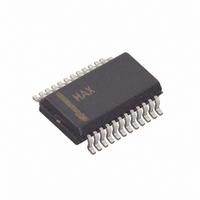
IC CNTRLR STP DWN 24-QSOP
Manufacturer
Maxim Integrated Products
Type
Step-Down (Buck)r
Datasheet
1.MAX8650EEG.pdf
(25 pages)
Specifications of MAX8650EEG+
Internal Switch(s)
No
Synchronous Rectifier
No
Number Of Outputs
1
Voltage - Output
0.7 ~ 5.5 V
Current - Output
25A
Frequency - Switching
200kHz ~ 1.2MHz
Voltage - Input
4.5 ~ 28 V
Operating Temperature
-40°C ~ 85°C
Mounting Type
Surface Mount
Package / Case
24-QSOP
Power - Output
762mW
Output Voltage
0.7 V to 5.5 V
Output Current
25 A
Input Voltage
4.5 V to 28 V
Mounting Style
SMD/SMT
Maximum Operating Temperature
+ 85 C
Minimum Operating Temperature
- 40 C
Lead Free Status / RoHS Status
Lead free / RoHS Compliant


4.5V to 28V Input Current-Mode Step-Down
Controller with Adjustable Frequency
Use R
where V
the dead time between high-side and low-side switching
transitions (30ns typ), and f
The high-side MOSFET operates as a duty-cycle con-
trol switch and has the following major losses: the
channel-conduction loss (P
switching loss (P
The high-side MOSFET does not have body-diode con-
duction loss, unless the converter is sinking current,
when the loss due to body-diode conduction is calcu-
lated as P
Use R
where I
capability determined by:
where R
on-resistance (1.5Ω typ) and R
resistance of the MOSFET (~2Ω):
where V
In addition to the losses above, allow approximately
20% more for additional losses due to MOSFET output
capacitances and low-side MOSFET body-diode
reverse-recovery charge dissipated in the high-side
MOSFET, but is not well defined in the MOSFET data
sheet. Refer to the MOSFET data sheet for thermal-
resistance specifications to calculate the PCB area
needed to maintain the desired maximum operating
20
______________________________________________________________________________________
P
HSDR
DS(ON)
DS(ON)
GATE
F
GS
P
DS(ON)(DR)
P
HSSW
is the body-diode forward-voltage drop, t
HSDC
LSCC
P
≈ V
=
HSCC
P
I
LSDC
GATE
at T
at T
Q
is the average DH driver output-current
VL.
G
=
=
= 2 x I
J(MAX)
J(MAX)
⎛
⎜
⎝
V
×
HSSW
=
1
IN
= ×
≅
V
−
V
2
GS
is the high-side MOSFET driver’s
R
×
OUT
V
V
LOAD
IN
DS ON DR
OUT
V
I
LOAD
IN
:
I
:
), and the drive loss (P
LOAD
×
(
f
S
×
S
⎞
⎟ ×
⎠
0 5 .
I
is the switching frequency.
HSCC
x V
×
2
LOAD
)(
×
I
×
R
2
LOAD
×
Q
GATE
F
GATE
V
V
)
F
GS
x t
VL
), the VL overlapping
I
+
×
×
GATE
DT
R
×
t
R
+
DT
GATE
is the internal gate
R
+
R
DS ON
Q
x f
GATE
DS ON
R
GD
×
(
DS ON DR
S
f
(
S
:
(
×
)
)
f
S
)(
HSDR
)
DT
is
).
junction temperature with the above calculated power
dissipations.
To reduce EMI caused by switching noise, add a 0.1µF
ceramic capacitor from the high-side switch drain to
the low-side switch source or add resistors in series
with DH and DL to slow down the switching transitions.
However, adding series resistors increases the power
dissipation of the MOSFET, so ensure this does not
overheat the MOSFET.
The input filter capacitor reduces peak currents drawn
from the power source and reduces noise and voltage
ripple on the input caused by the circuit’s switching.
The input capacitor must meet the ripple-current
requirement (I
defined by the following equation:
I
equals twice the output voltage (V
I
mended due to their low ESR and ESL at high frequen-
cy with relatively low cost. Choose a capacitor that
exhibits less than 10°C temperature rise at the maxi-
mum operating RMS current for optimum long-term reli-
ability. Ceramic capacitors with X5R or better
temperature characteristics are recommended.
The key selection parameters for the output capacitor
are the actual capacitance value, the equivalent series
resistance (ESR), the equivalent series inductance
(ESL), and the voltage-rating requirements. These
parameters affect the overall stability, output voltage
ripple, and transient response. The output ripple has
three components: variations in the charge stored in
the output capacitor, the voltage drop across the
capacitor’s ESR and ESL caused by the current into
and out of the capacitor. The maximum output voltage
ripple is estimated as follows:
The output voltage ripple as a consequence of the
ESR, ESL, and output capacitance is:
RMS
RMS(MAX)
V
RIPPLE
has a maximum value when the input voltage
= V
= I
I
RMS
V
LOAD
RIPPLE(ESR)
RIPPLE ESL
RMS
V
RIPPLE ESR
=
) imposed by the switching currents
I
LOAD
/ 2. Ceramic capacitors are recom-
(
(
)
+ V
=
V
)
OUT
=
L ESL
I
RIPPLE(C)
+
P P
V
V
IN
−
IN
×
Output Capacitor
(
×
V
IN
Input Capacitor
ESR
×
IN
ESL
−
= 2 x V
+ V
V
OUT
RIPPLE(ESL)
)
OUT
), so
Related parts for MAX8650EEG+
Image
Part Number
Description
Manufacturer
Datasheet
Request
R

Part Number:
Description:
MAX7528KCWPMaxim Integrated Products [CMOS Dual 8-Bit Buffered Multiplying DACs]
Manufacturer:
Maxim Integrated Products
Datasheet:
Part Number:
Description:
Single +5V, fully integrated, 1.25Gbps laser diode driver.
Manufacturer:
Maxim Integrated Products
Datasheet:
Part Number:
Description:
Single +5V, fully integrated, 155Mbps laser diode driver.
Manufacturer:
Maxim Integrated Products
Datasheet:
Part Number:
Description:
VRD11/VRD10, K8 Rev F 2/3/4-Phase PWM Controllers with Integrated Dual MOSFET Drivers
Manufacturer:
Maxim Integrated Products
Datasheet:
Part Number:
Description:
Highly Integrated Level 2 SMBus Battery Chargers
Manufacturer:
Maxim Integrated Products
Datasheet:
Part Number:
Description:
Current Monitor and Accumulator with Integrated Sense Resistor; ; Temperature Range: -40°C to +85°C
Manufacturer:
Maxim Integrated Products
Part Number:
Description:
TSSOP 14/A�/RS-485 Transceivers with Integrated 100O/120O Termination Resis
Manufacturer:
Maxim Integrated Products
Part Number:
Description:
TSSOP 14/A�/RS-485 Transceivers with Integrated 100O/120O Termination Resis
Manufacturer:
Maxim Integrated Products
Part Number:
Description:
QFN 16/A�/AC-DC and DC-DC Peak-Current-Mode Converters with Integrated Step
Manufacturer:
Maxim Integrated Products
Part Number:
Description:
TDFN/A/65V, 1A, 600KHZ, SYNCHRONOUS STEP-DOWN REGULATOR WITH INTEGRATED SWI
Manufacturer:
Maxim Integrated Products
Part Number:
Description:
Integrated Temperature Controller f
Manufacturer:
Maxim Integrated Products
Part Number:
Description:
SOT23-6/I�/45MHz to 650MHz, Integrated IF VCOs with Differential Output
Manufacturer:
Maxim Integrated Products
Part Number:
Description:
SOT23-6/I�/45MHz to 650MHz, Integrated IF VCOs with Differential Output
Manufacturer:
Maxim Integrated Products
Part Number:
Description:
EVALUATION KIT/2.4GHZ TO 2.5GHZ 802.11G/B RF TRANSCEIVER WITH INTEGRATED PA
Manufacturer:
Maxim Integrated Products
Part Number:
Description:
QFN/E/DUAL PCIE/SATA HIGH SPEED SWITCH WITH INTEGRATED BIAS RESISTOR
Manufacturer:
Maxim Integrated Products
Datasheet: