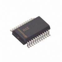
MAX8650EEG+ Maxim Integrated Products, MAX8650EEG+ Datasheet - Page 24

MAX8650EEG+
Manufacturer Part Number
MAX8650EEG+
Description
IC CNTRLR STP DWN 24-QSOP
Manufacturer
Maxim Integrated Products
Type
Step-Down (Buck)r
Datasheet
1.MAX8650EEG.pdf
(25 pages)
Specifications of MAX8650EEG+
Internal Switch(s)
No
Synchronous Rectifier
No
Number Of Outputs
1
Voltage - Output
0.7 ~ 5.5 V
Current - Output
25A
Frequency - Switching
200kHz ~ 1.2MHz
Voltage - Input
4.5 ~ 28 V
Operating Temperature
-40°C ~ 85°C
Mounting Type
Surface Mount
Package / Case
24-QSOP
Power - Output
762mW
Output Voltage
0.7 V to 5.5 V
Output Current
25 A
Input Voltage
4.5 V to 28 V
Mounting Style
SMD/SMT
Maximum Operating Temperature
+ 85 C
Minimum Operating Temperature
- 40 C
Lead Free Status / RoHS Status
Lead free / RoHS Compliant
Careful PCB layout is critical to achieve low switching
losses and clean, stable operation. The switching power
stage requires particular attention. Follow these guide-
lines for good PCB layout:
1) Place IC decoupling capacitors as close to IC pins
2) For output current greater than 10A, a multilayer
3) Connect input, output, and VL capacitors to the
4) Place the inductor current-sense resistor and capac-
5) Place the MOSFET as close as possible to the IC to
6) Connect the drain leads of the power MOSFET to a
4.5V to 28V Input Current-Mode Step-Down
Controller with Adjustable Frequency
24
as possible. Keep the power ground plane and sig-
nal ground plane separate. Place the input ceramic
decoupling capacitor directly across and as close as
possible to the high-side MOSFET’s drain and the
low-side MOSFET’s source. This is to help contain
the high switching current within this small loop.
PCB is recommended. Pour a signal ground plane
in the second layer underneath the IC to minimize
noise coupling.
power ground plane; connect all other capacitors to
the signal ground plane.
itor as close to the inductor as possible. Make a
Kelvin connection to minimize the effect of PCB trace
resistance. Place the input-bias balance resistor (R5
in Figures 8 and 9) near CS-. Run two closely paral-
lel traces from across the capacitor (C9 in Figures 8
and 9) to CS+ and CS-.
minimize trace inductance of the gate-drive loop. If
parallel MOSFETs are used, keep the trace lengths
to both gates equal.
large copper area to help cool the device. Refer to
______________________________________________________________________________________
Applications Information
PCB Layout Guidelines
7) Place the feedback and compensation components
8) Refer to the MAX8650 evaluation kit for an example
PROCESS: BiCMOS
For the latest package outline information and land patterns, go
to www.maxim-ic.com/packages.
PACKAGE TYPE
the power MOSFET data sheet for recommended
copper area.
as close to the IC pins as possible. Connect the
feedback resistor-divider from FB to the output as
close as possible to the farthest output capacitor.
layout.
24 QSOP
TOP VIEW
SYNCO
FSYNC
MODE
PGND
BST
AVL
DH
DL
EN
LX
VL
IN
PACKAGE CODE
10
11
12
1
2
3
4
5
6
7
8
9
Package Information
+
E24-1
MAX8650
QSOP
Pin Configuration
Chip Information
24
23
22
21
20
19
18
17
16
15
14
13
DOCUMENT NO.
POK
SCOMP
ILIM2
REFIN
SS
COMP
FB
OVP
ILIM1
CS-
CS+
GND
21-0055


