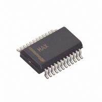
MAX8650EEG+ Maxim Integrated Products, MAX8650EEG+ Datasheet - Page 2

MAX8650EEG+
Manufacturer Part Number
MAX8650EEG+
Description
IC CNTRLR STP DWN 24-QSOP
Manufacturer
Maxim Integrated Products
Type
Step-Down (Buck)r
Datasheet
1.MAX8650EEG.pdf
(25 pages)
Specifications of MAX8650EEG+
Internal Switch(s)
No
Synchronous Rectifier
No
Number Of Outputs
1
Voltage - Output
0.7 ~ 5.5 V
Current - Output
25A
Frequency - Switching
200kHz ~ 1.2MHz
Voltage - Input
4.5 ~ 28 V
Operating Temperature
-40°C ~ 85°C
Mounting Type
Surface Mount
Package / Case
24-QSOP
Power - Output
762mW
Output Voltage
0.7 V to 5.5 V
Output Current
25 A
Input Voltage
4.5 V to 28 V
Mounting Style
SMD/SMT
Maximum Operating Temperature
+ 85 C
Minimum Operating Temperature
- 40 C
Lead Free Status / RoHS Status
Lead free / RoHS Compliant
ABSOLUTE MAXIMUM RATINGS
IN, EN to GND ........................................................-0.3V to +30V
BST to LX...............................................................-0.3V to +7.5V
DH to LX ....................................................-0.3V to (V
LX to GND .................... -1V (-2.5V for < 50ns transient) to +30V
DL to PGND.................................................-0.3V to (V
ILIM2, ILIM1, SYNCO, FSYNC, OVP,
VL to PGND ...........................................................-0.3V to +7.5V
4.5V to 28V Input Current-Mode Step-Down
Controller with Adjustable Frequency
Stresses beyond those listed under “Absolute Maximum Ratings” may cause permanent damage to the device. These are stress ratings only, and functional
operation of the device at these or any other conditions beyond those indicated in the operational sections of the specifications is not implied. Exposure to
absolute maximum rating conditions for extended periods may affect device reliability.
ELECTRICAL CHARACTERISTICS
(V
Dual Mode is a trademark of Maxim Integrated Products, Inc.
2
Operating Input Voltage Range
Quiescent Supply Current
Shutdown Supply Current
I
AVL Undervoltage-Lockout Trip
Level
Output Voltage Adjust Range
VL Regulation Voltage
VL Output Current
AVL Regulation Voltage
AVL Output Current
SOFT-START
SS Shutdown Resistance
SS Soft-Start Current
REFIN INPUT
REFIN Dual Mode™ Threshold
REFIN Input Bias Current
REFIN Input Voltage Range
IN
SCOMP to GND .....................................-0.3V to (V
IN
+ I
_______________________________________________________________________________________
= 12V, V
VL
+ I
PARAMETER
AVL
BST
- V
LX
= 6.5V, T
A
= -40°C to +85°C. Typical values are at T
VL = IN for V
V
EN = GND, V
EN = GND, V
V
Minimum output voltage is limited by minimum duty cycle
and external components
7V < V
5.5V < V
From SS to GND, V
V
V
FB
AVL
SS
REFIN
= 0.75V, no switching
= 0.625V
rising, 3% typ hysteresis
IN
= 0.7V to 1.5V
VL
< 28V, 1mA < I
< 7V, 1mA < I
IN
IN
AVL
AVL
BST
< 7V
≤ 28V
VL
= V
EN
+ 0.3V)
+ 0.3V)
+ 0.3V)
VL
CONDITIONS
= 0V
= V
LOAD
LOAD
IN
= 5V
< 40mA
< 10mA
AVL, FB, POK, COMP, SS, MODE, REFIN to GND .....-0.3V to +6V
CS+, CS- to GND .....................................................-0.3V to +6V
PGND to GND .......................................................-0.3V to +0.3V
Continuous Power Dissipation (T
Junction Temperature ......................................................+150°C
Storage Temperature Range .............................-65°C to +150°C
Lead Temperature (soldering, 10s) .................................+300°C
24-Pin QSOP (derate 9.5mW/°C above +70°C)..........762mW
A
= +25°C, unless otherwise noted.) (Note 1)
V
4.900
3.90
1.0V
-250
MIN
AVL
4.5
0.7
6.0
40
10
18
0
A
-
= +70°C)
4.975
TYP
4.15
6.5
20
23
2
5.050
+250
MAX
V
28.0
4.40
100
5.5
7.0
1.5
10
32
28
AVL
3
UNITS
mA
mA
mA
µA
µA
nA
Ω
V
V
V
V
V
V
V


