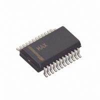
MAX8650EEG+ Maxim Integrated Products, MAX8650EEG+ Datasheet - Page 21

MAX8650EEG+
Manufacturer Part Number
MAX8650EEG+
Description
IC CNTRLR STP DWN 24-QSOP
Manufacturer
Maxim Integrated Products
Type
Step-Down (Buck)r
Datasheet
1.MAX8650EEG.pdf
(25 pages)
Specifications of MAX8650EEG+
Internal Switch(s)
No
Synchronous Rectifier
No
Number Of Outputs
1
Voltage - Output
0.7 ~ 5.5 V
Current - Output
25A
Frequency - Switching
200kHz ~ 1.2MHz
Voltage - Input
4.5 ~ 28 V
Operating Temperature
-40°C ~ 85°C
Mounting Type
Surface Mount
Package / Case
24-QSOP
Power - Output
762mW
Output Voltage
0.7 V to 5.5 V
Output Current
25 A
Input Voltage
4.5 V to 28 V
Mounting Style
SMD/SMT
Maximum Operating Temperature
+ 85 C
Minimum Operating Temperature
- 40 C
Lead Free Status / RoHS Status
Lead free / RoHS Compliant
where I
These equations are suitable for initial capacitor selec-
tion, but final values should be chosen based on a proto-
type or evaluation circuit. As a general rule, a smaller
current ripple results in less output-voltage ripple. Since
the inductor ripple current is a factor of the inductor
value and input voltage, the output-voltage ripple
decreases with larger inductance, and increases with
higher input voltages. Ceramic, tantalum, or aluminum
polymer electrolytic capacitors are recommended. The
aluminum electrolytic capacitor is the least expensive;
however, it has higher ESR. To compensate for this, use
a ceramic capacitor in parallel to reduce the switching
ripple and noise. For reliable and safe operation, ensure
that the capacitor’s voltage and ripple-current ratings
exceed the calculated values.
The response to a load transient depends on the
selected output capacitors. After a load transient, the
output voltage instantly changes by ESR x ΔI
Before the controller can respond, the output voltage
deviates further, depending on the inductor and output-
capacitor values. After a short period (see the Typical
Operating Characteristics ), the controller responds by
regulating the output voltage back to its nominal state.
The controller response time depends on its closed-
loop bandwidth. With a higher bandwidth, the response
time is faster, thus preventing the output voltage from
further deviation from its regulating value.
The MAX8650 uses an internal transconductance error
amplifier whose output compensates the control loop.
The external inductor, output capacitor, compensation
resistor, and compensation capacitors determine the
loop stability. The inductor and output capacitor are
chosen based on performance, size, and cost.
Additionally, the compensation resistor and capacitors
are selected to optimize control-loop stability. The com-
ponent values, shown in the circuits of Figures 3 and 4,
yield stable operation over the given range of input-to-
output voltages.
The controller uses a current-mode control scheme that
regulates the output voltage by forcing the required cur-
rent through the external inductor, so the MAX8650 uses
the voltage drop across the DC resistance of the induc-
P-P
is the peak-to-peak inductor current:
4.5V to 28V Input Current-Mode Step-Down
V
I
P P
RIPPLE C
−
______________________________________________________________________________________
=
V
( )
IN
f
S
−
=
Controller with Adjustable Frequency
×
V
8
Compensation Design
OUT
L
×
C
I
P P
OUT
×
−
V
OUT
V
×
IN
f
S
LOAD
.
tor or the alternate series current-sense resistor to mea-
sure the inductor current. Current-mode control elimi-
nates the double pole in the feedback loop caused by
the inductor and output capacitor resulting in a smaller
phase shift and requiring a less elaborate error-amplifier
compensation than voltage-mode control. A simple sin-
gle-series R
ble, high-bandwidth loop in applications where ceramic
capacitors are used for output filtering. For other types
of capacitors, due to the higher capacitance and ESR,
the frequency of the zero created by the capacitance
and ESR is lower than the desired closed-loop
crossover frequency. To stabilize a nonceramic output
capacitor loop, add another compensation capacitor
from COMP to GND to cancel this ESR zero.
The basic regulator loop is modeled as a power modu-
lator, an output feedback-divider, and an error amplifi-
er. The power modulator has DC gain set by g
R
put capacitor (C
that define the power modulator:
where R
frequency, L is the output inductance, and g
(A
sense amplifier (12 typ), and R
of the inductor.
Find the pole and zero frequencies created by the
power modulator as follows:
When C
lel, the resulting C
ESR
lel combination of like capacitors is the same as for an
individual capacitor. See Figures 10 and 11 for illustra-
tions of the pole and zero locations.
The feedback voltage-divider has a gain of G
V
OUT
LOAD
VCS
(EACH)
f
, where V
pMOD
, with a pole and zero pair set by R
x R
OUT
LOAD
DC
G
/ n. Note that the capacitor zero for a paral-
C
=
comprises “n” identical capacitors in paral-
MOD dc
), where A
and C
2π
f
zMOD
FB
= V
OUT
×
(
is equal to 0.75V.
OUT
C
OUT
C
OUT
), and its ESR. Below are equations
)
=
=
is all that is needed to have a sta-
2π
g
/ I
= n x C
VCS
mc
×
OUT(MAX)
×
⎛
⎜
⎝
C
R
R
×
is the gain of the current-
OUT
LOAD
LOAD
R
R
1
1
DC
LOAD
LOAD
OUT(EACH)
×
is the DC resistance
, f
×
+
ESR
f
f
S
S
S
×
+
f
f
×
×
is the switching
S
S
L
L
LOAD
×
×
, and ESR =
+
L
L
ESR
FB
, the out-
mc
= V
⎞
⎟
⎠
= 1 /
mc
FB
21
x
/


