AC162078 Microchip Technology, AC162078 Datasheet - Page 59
AC162078
Manufacturer Part Number
AC162078
Description
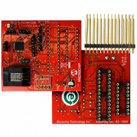
HEADER INTRFC MPLAB ICD2 18F1330
Manufacturer
Microchip Technology
Datasheet
1.AC162078.pdf
(318 pages)
Specifications of AC162078
Accessory Type
Transition Header
Lead Free Status / RoHS Status
Not applicable / Not applicable
For Use With/related Products
ICD2
Lead Free Status / RoHS Status
Lead free / RoHS Compliant, Not applicable / Not applicable
Available stocks
Company
Part Number
Manufacturer
Quantity
Price
Company:

Part Number:
AC162078
Manufacturer:
MICROCHIP
Quantity:
12 000


FIGURE 6-6:
6.3.2
While the use of the BSR with an embedded 8-bit
address allows users to address the entire range of
data memory, it also means that the user must always
ensure that the correct bank is selected. Otherwise,
data may be read from or written to the wrong location.
This can be disastrous if a GPR is the intended target
of an operation, but an SFR is written to instead.
Verifying and/or changing the BSR for each read or
write to data memory can become very inefficient.
To streamline access for the most commonly used data
memory locations, the data memory is configured with
an Access Bank, which allows users to access a
mapped block of memory without specifying a BSR.
The Access Bank consists of the first 128 bytes of
memory (00h-7Fh) in Bank 0 and the last 128 bytes of
memory (80h-FFh) in Block 15. The lower half is known
as the “Access RAM” and is composed of GPRs. The
upper half is where the device’s SFRs are mapped.
These two areas are mapped contiguously in the
Access Bank and can be addressed in a linear fashion
by an 8-bit address (Figure 6-5).
The Access Bank is used by core PIC18 instructions
that include the Access RAM bit (the ‘a’ parameter in
the instruction). When ‘a’ is equal to ‘1’, the instruction
uses the BSR and the 8-bit address included in the
opcode for the data memory address. When ‘a’ is ‘0’,
2009 Microchip Technology Inc.
Note 1:
Bank Select
7
0
ACCESS BANK
2:
0
0 0
The Access RAM bit of the instruction can be used to force an override of the selected bank (BSR<3:0>) to
the registers of the Access Bank.
The MOVFF instruction embeds the entire 12-bit address in the instruction.
(2)
BSR
USE OF THE BANK SELECT REGISTER (DIRECT ADDRESSING)
0
(1)
0 0
0
0
E00h
FFFh
F00h
000h
100h
Data Memory
Bank 13
Bank 14
Bank 15
through
Bank 0
Bank 1
however, the instruction is forced to use the Access
Bank address map; the current value of the BSR is
ignored entirely.
Using this “forced” addressing allows the instruction to
operate on a data address in a single cycle without
updating the BSR first. For 8-bit addresses of 80h and
above, this means that users can evaluate and operate
on SFRs more efficiently. The Access RAM below 80h
is a good place for data values that the user might need
to access rapidly, such as immediate computational
results or common program variables. Access RAM
also allows for faster and more code efficient context
saving and switching of variables.
The mapping of the Access Bank is slightly different
when the extended instruction set is enabled (XINST
Configuration bit = 1). This is discussed in more detail
in Section 6.5.3 “Mapping the Access Bank in
Indexed Literal Offset Addressing Mode”.
6.3.3
PIC18 devices may have banked memory in the GPR
area. This is data RAM which is available for use by all
instructions. GPRs start at the bottom of Bank 0
(address 000h) and grow upwards towards the bottom of
the SFR area. GPRs are not initialized by a Power-on
Reset and are unchanged on all other Resets.
00h
FFh
00h
FFh
00h
FFh
00h
FFh
PIC18F1230/1330
GENERAL PURPOSE
REGISTER FILE
7
1
1
From Opcode
1
1
1
1
DS39758D-page 59
(2)
1
1
0
Related parts for AC162078
Image
Part Number
Description
Manufacturer
Datasheet
Request
R

Part Number:
Description:
Manufacturer:
Microchip Technology Inc.
Datasheet:
Part Number:
Description:
Manufacturer:
Microchip Technology Inc.
Datasheet:
Part Number:
Description:
Manufacturer:
Microchip Technology Inc.
Datasheet:
Part Number:
Description:
Manufacturer:
Microchip Technology Inc.
Datasheet:
Part Number:
Description:
Manufacturer:
Microchip Technology Inc.
Datasheet:
Part Number:
Description:
Manufacturer:
Microchip Technology Inc.
Datasheet:
Part Number:
Description:
Manufacturer:
Microchip Technology Inc.
Datasheet:
Part Number:
Description:
Manufacturer:
Microchip Technology Inc.
Datasheet: