AC162078 Microchip Technology, AC162078 Datasheet - Page 87
AC162078
Manufacturer Part Number
AC162078
Description
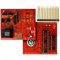
HEADER INTRFC MPLAB ICD2 18F1330
Manufacturer
Microchip Technology
Datasheet
1.AC162078.pdf
(318 pages)
Specifications of AC162078
Accessory Type
Transition Header
Lead Free Status / RoHS Status
Not applicable / Not applicable
For Use With/related Products
ICD2
Lead Free Status / RoHS Status
Lead free / RoHS Compliant, Not applicable / Not applicable
Available stocks
Company
Part Number
Manufacturer
Quantity
Price
Company:

Part Number:
AC162078
Manufacturer:
MICROCHIP
Quantity:
12 000


10.0
Depending on the device selected and features
enabled, there are up to five ports available. Some pins
of the I/O ports are multiplexed with an alternate
function from the peripheral features on the device. In
general, when a peripheral is enabled, that pin may not
be used as a general purpose I/O pin.
Each port has three registers for its operation. These
registers are:
• TRIS register (Data Direction register)
• PORT register (reads the levels on the pins of the
• LAT register (Output Latch register)
The Output Latch (LAT register) is useful for read-
modify-write operations on the value that the I/O pins
are driving.
A simplified model of a generic I/O port, without the
interfaces to other peripherals, is shown in Figure 10-1.
FIGURE 10-1:
10.1
PORTA is an 8-bit wide, bidirectional port. The
corresponding Data Direction register is TRISA. Setting
a TRISA bit (= 1) will make the corresponding PORTA
pin an input (i.e., put the corresponding output driver in
a high-impedance mode). Clearing a TRISA bit (= 0)
will make the corresponding PORTA pin an output (i.e.,
put the contents of the output latch on the selected pin).
2009 Microchip Technology Inc.
device)
Note 1:
RD LAT
Data
Bus
WR LAT
or Port
WR TRIS
RD TRIS
RD Port
I/O PORTS
PORTA, TRISA and LATA Registers
I/O pins have diode protection to V
TRIS Latch
Data Latch
D
D
CK
CK
GENERIC I/O PORT
OPERATION
Q
Q
Q
EN
EN
D
DD
and V
I/O pin
SS
Input
Buffer
.
(1)
Reading the PORTA register reads the status of the
pins, whereas writing to it, will write to the port latch.
The Output Latch (LATA) register is also memory
mapped. Read-modify-write operations on the LATA
register read and write the latched output value for
PORTA.
Pins RA6 and RA7 are multiplexed with the main
oscillator pins; they are enabled as oscillator or I/O pins
by the selection of the main oscillator in the Configura-
tion register (see Section 20.1 “Configuration Bits”
for details). When they are not used as port pins, RA6
and RA7 and their associated TRIS and LAT bits are
read as ‘0’.
The RA0 pin is multiplexed with one of the analog
inputs, one of the external interrupt inputs, one of the
interrupt-on-change inputs and one of the analog
comparator inputs to become RA0/AN0/INT0/KBI0/
CMP0 pin.
The RA1 pin is multiplexed with one of the analog
inputs, one of the external interrupt inputs and one of
the interrupt-on-change inputs to become RA1/AN1/
INT1/KBI1 pin.
Pins RA2 and RA3 are multiplexed with the Enhanced
USART transmission and reception input (see
Section 20.1 “Configuration Bits” for details).
The RA4 pin is multiplexed with the Timer0 module
clock input, one of the analog inputs and the analog
V
The Fault detect input for PWM FLTA is multiplexed with
pins RA5 and RA7. Its placement is decided by clearing
or setting the FLTAMX bit of Configuration Register 3H.
The TRISA register controls the direction of the PORTA
pins, even when they are being used as analog inputs.
The user must ensure the bits in the TRISA register are
maintained set when using them as analog inputs.
EXAMPLE 10-1:
CLRF
CLRF
MOVLW
MOVWF
MOVWF
MOVWF
MOVLW
MOVWF
REF
Note:
+ input to become the RA4/T0CKI/AN2/V
PIC18F1230/1330
PORTA
LATA
07h
ADCON1 ; for digital inputs
07h
CMCON
0CFh
TRISA
On a Power-on Reset, RA0, RA1, RA4
and RA5 are configured as analog inputs
and read as ‘0’. RA2 and RA3 are
configured as digital inputs.
; Initialize PORTA by
; clearing output
; data latches
; Alternate method
; to clear output
; data latches
; Configure A/D
; Configure comparators
; for digital input
; Value used to
; initialize data
; direction
; Set RA<7:6,3:0> as inputs
; RA<5:4> as outputs
INITIALIZING PORTA
DS39758D-page 87
REF
+ pin.
Related parts for AC162078
Image
Part Number
Description
Manufacturer
Datasheet
Request
R

Part Number:
Description:
Manufacturer:
Microchip Technology Inc.
Datasheet:
Part Number:
Description:
Manufacturer:
Microchip Technology Inc.
Datasheet:
Part Number:
Description:
Manufacturer:
Microchip Technology Inc.
Datasheet:
Part Number:
Description:
Manufacturer:
Microchip Technology Inc.
Datasheet:
Part Number:
Description:
Manufacturer:
Microchip Technology Inc.
Datasheet:
Part Number:
Description:
Manufacturer:
Microchip Technology Inc.
Datasheet:
Part Number:
Description:
Manufacturer:
Microchip Technology Inc.
Datasheet:
Part Number:
Description:
Manufacturer:
Microchip Technology Inc.
Datasheet: