CDB5376 Cirrus Logic Inc, CDB5376 Datasheet - Page 18
CDB5376
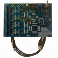
Manufacturer Part Number
CDB5376
Description
EVALUATION BOARD FOR CS5376
Manufacturer
Cirrus Logic Inc
Datasheets
1.CS5371A-ISZR.pdf
(32 pages)
2.CS4373A-ISZ.pdf
(34 pages)
3.CS5376A-IQZR.pdf
(106 pages)
4.CDB5378.pdf
(16 pages)
5.CDB5376.pdf
(80 pages)
6.CDB5376.pdf
(16 pages)
Specifications of CDB5376
Main Purpose
Seismic Evaluation System
Embedded
Yes, MCU, 8-Bit
Utilized Ic / Part
CS3301A, CS3302A, CS4373A, CS5372A, CS5376A
Primary Attributes
Quad Digital Filter
Secondary Attributes
Graphical User Interface, SPI™ & USB Interfaces
Processor To Be Evaluated
CS330x, CS4373A, CS537x
Interface Type
USB
Lead Free Status / RoHS Status
Contains lead / RoHS non-compliant
Lead Free Status / RoHS Status
Lead free / RoHS Compliant, Contains lead / RoHS non-compliant
Other names
598-1778


5. DIGITAL SIGNALS
The CS5371A and CS5372A modulators are
designed to operate with the CS5376A digital
filter. The digital filter generates the modulator
clock and synchronization signals (MCLK and
MSYNC) while receiving back the modulator
one-bit ΔΣ conversion data and over-range
flag (MDATA and MFLAG).
5.1 MCLK Connection
The CS5376A digital filter generates the mas-
ter clock for CS5371A and CS5372A, typically
2.048 MHz, from a synchronous clock input
from the external system. If MCLK is disabled
during operation, the modulators will enter a
power down state after approximately 40
By default, MCLK is disabled at reset and is
enabled by writing the digital filter CONFIG
register.
MCLK must have low jitter to guarantee full an-
alog performance, requiring a crystal- or
VCXO-based system clock input to the digital
18
VA+
VA+
VA-
VA-
VA+
VA+
VA-
VA-
AMPLIFIER
AMPLIFIER
CS3301A
CS3302A
CS3301A
CS3302A
VA+
VA-
OUTR+
OUTF+
OUTF-
OUTR-
OUTR+
OUTF+
OUTF-
OUTR-
VREF
2.5 V
680
680
680
680
680
680
680
680
10 Ω
100μF
20nF
20nF
C0G
C0G
Figure 12. Digital Signals
VA+
VA-
0.01μF
20nF
C0G
20nF
C0G
µ
S.
INR+
INF+
INF-
INR-
VREF+
VREF-
INR-
INF-
INF+
INR+
0.1μF
0.1μF
filter. Clock jitter on the digital filter CLK input
directly translates to jitter on MCLK.
5.2 MSYNC Connection
The CS5376A digital filter also provides a syn-
chronization signal to the CS5371A and
CS5372A modulators. The MSYNC signal is
automatically generated following a rising
edge received on the digital filter SYNC input.
By default, MSYNC generation is disabled at
reset and is enabled by writing the digital filter
CONFIG register.
The input SYNC signal to the CS5376A digital
filter sets a common reference time t
surement events, thereby synchronizing ana-
log sampling across a measurement network.
The timing accuracy of the received SYNC sig-
nal from measurement node to measurement
node must be ±1 MCLK to maximize the
MSYNC analog sample synchronization accu-
racy.
VA+
ΔΣ Modulator
VA-
CS5372A
GND
VD
MDATA2
MFLAG2
MDATA1
MFLAG1
MSYNC
PWDN2
PWDN1
0.01μF
MCLK
OFST
VD
CS5371A CS5372A
MDATA1
MFLAG1
GPIO
MCLK
MSYNC
GPIO
MDATA2
MFLAG2
GPIO
Digital Filter
CS5376A
VDD2
GND
VD
0
for mea-
DS748F3
Related parts for CDB5376
Image
Part Number
Description
Manufacturer
Datasheet
Request
R

Part Number:
Description:
Development Kit
Manufacturer:
Cirrus Logic Inc
Datasheet:
Part Number:
Description:
Development Kit
Manufacturer:
Cirrus Logic Inc
Datasheet:


Part Number:
Description:
High-efficiency PFC + Fluorescent Lamp Driver Reference Design
Manufacturer:
Cirrus Logic Inc
Datasheet:
Part Number:
Description:
Development Kit
Manufacturer:
Cirrus Logic Inc
Datasheet:
Part Number:
Description:
Development Kit
Manufacturer:
Cirrus Logic Inc
Datasheet:

Part Number:
Description:
Development Kit
Manufacturer:
Cirrus Logic Inc
Datasheet:
Part Number:
Description:
Development Kit
Manufacturer:
Cirrus Logic Inc
Datasheet:
Part Number:
Description:
Development Kit
Manufacturer:
Cirrus Logic Inc
Datasheet:
Part Number:
Description:
Development Kit
Manufacturer:
Cirrus Logic Inc
Datasheet:

Part Number:
Description:
EVALUATION BOARD FOR CS8427
Manufacturer:
Cirrus Logic Inc
Datasheet:

Part Number:
Description:
BOARD EVAL FOR CS8416 RCVR
Manufacturer:
Cirrus Logic Inc
Datasheet:

Part Number:
Description:
EVALUATION BOARD FOR CS8420
Manufacturer:
Cirrus Logic Inc
Datasheet:

Part Number:
Description:
KIT DEVELOPMENT EP9315 ARM9
Manufacturer:
Cirrus Logic Inc
Datasheet:

Part Number:
Description:
KIT DEVELOPMENT EP9302 ARM9
Manufacturer:
Cirrus Logic Inc
Datasheet: