CDB5376 Cirrus Logic Inc, CDB5376 Datasheet - Page 4
CDB5376
Manufacturer Part Number
CDB5376
Description
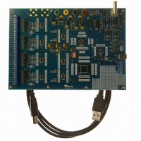
EVALUATION BOARD FOR CS5376
Manufacturer
Cirrus Logic Inc
Datasheets
1.CS5371A-ISZR.pdf
(32 pages)
2.CS4373A-ISZ.pdf
(34 pages)
3.CS5376A-IQZR.pdf
(106 pages)
4.CDB5378.pdf
(16 pages)
5.CDB5376.pdf
(80 pages)
6.CDB5376.pdf
(16 pages)
Specifications of CDB5376
Main Purpose
Seismic Evaluation System
Embedded
Yes, MCU, 8-Bit
Utilized Ic / Part
CS3301A, CS3302A, CS4373A, CS5372A, CS5376A
Primary Attributes
Quad Digital Filter
Secondary Attributes
Graphical User Interface, SPI™ & USB Interfaces
Processor To Be Evaluated
CS330x, CS4373A, CS537x
Interface Type
USB
Lead Free Status / RoHS Status
Contains lead / RoHS non-compliant
Lead Free Status / RoHS Status
Lead free / RoHS Compliant, Contains lead / RoHS non-compliant
Other names
598-1778


1. CHARACTERISTICS AND SPECIFICATIONS
•
•
•
•
SPECIFIED OPERATING CONDITIONS
Notes: 1. VA- must always be the most-negative input voltage to avoid potential SCR latch-up conditions.
ABSOLUTE MAXIMUM RATINGS
Notes: 5. Transient currents up to ±100 mA will not cause SCR latch-up.
4
WARNING: Operation at or beyond these limits may result in permanent damage to the device.
Bipolar Power Supplies
Positive Analog
Negative Analog
Positive Digital
Voltage Reference
[VREF+] - [VREF-]
VREF-
Thermal
Ambient Operating Temperature
DC Power Supplies
Analog Supply Differential
Digital Supply Differential
Input Current, Power Supplies
Input Current, Any Pin Except Supplies
Output Current
Power Dissipation
Analog Input Voltages
Digital Input Voltages
Storage Temperature Range
Min / Max characteristics and specifications are guaranteed over the
Typical performance characteristics and specifications are measured at nominal supply voltages and T
GND = 0 V. Single-ended voltages with respect to GND, differential voltages with respect to opposite half.
Device is connected as shown in
2. By design, a 2.500 V voltage reference input results in the best signal-to-noise performance.
3. Channel-to-channel gain accuracy is directly proportional to the voltage reference absolute accuracy.
4. VREF inputs must satisfy: VA- ≤ VREF- < VREF+ ≤ VA+.
6. Includes continuous over-voltage conditions at the modulator analog input pins.
Normal operation is not guaranteed at these extremes.
Parameter
Parameter
Figure 9 on page 13
Negative Analog
Positive Analog
(VA+) - (VA-)
(VD) - (VA-)
(Note 5,
Industrial (-ISZ)
(Note
(Note
(Note
Digital
(Note 2,
(Note
1) ± 2%
5)
6)
5)
± 3%
± 2%
unless otherwise noted.
Symbol
3)
4)
VD
VA
T
I
PDN
V
V
I
VA+
VA-
PWR
VD
OUT
I
STG
IND
INA
DIFF
IN
DIFF
Symbol
VREF-
VREF
VA+
VA-
VD
T
A
(VA-) - 0.5
Specified Operating
Min
-0.5
-6.8
-0.5
-0.5
-65
-2.45
3.20
-
-
-
-
-
-
2.45
Min
-40
-
-
CS5371A CS5372A
(VA+) + 0.5
2.500
(VD) + 0.5
Nom
-2.50
2.50
3.30
VA -
25
Max
±50
±10
±25
500
150
6.8
0.5
6.8
6.8
6.8
Conditions.
-2.55
Max
2.55
3.40
85
-
-
Parameter
mW
mA
mA
mA
ºC
DS748F3
A
V
V
V
V
V
V
V
= 25°C.
Unit
°C
V
V
V
V
V
Related parts for CDB5376
Image
Part Number
Description
Manufacturer
Datasheet
Request
R

Part Number:
Description:
Development Kit
Manufacturer:
Cirrus Logic Inc
Datasheet:
Part Number:
Description:
Development Kit
Manufacturer:
Cirrus Logic Inc
Datasheet:


Part Number:
Description:
High-efficiency PFC + Fluorescent Lamp Driver Reference Design
Manufacturer:
Cirrus Logic Inc
Datasheet:
Part Number:
Description:
Development Kit
Manufacturer:
Cirrus Logic Inc
Datasheet:
Part Number:
Description:
Development Kit
Manufacturer:
Cirrus Logic Inc
Datasheet:

Part Number:
Description:
Development Kit
Manufacturer:
Cirrus Logic Inc
Datasheet:
Part Number:
Description:
Development Kit
Manufacturer:
Cirrus Logic Inc
Datasheet:
Part Number:
Description:
Development Kit
Manufacturer:
Cirrus Logic Inc
Datasheet:
Part Number:
Description:
Development Kit
Manufacturer:
Cirrus Logic Inc
Datasheet:

Part Number:
Description:
EVALUATION BOARD FOR CS8427
Manufacturer:
Cirrus Logic Inc
Datasheet:

Part Number:
Description:
BOARD EVAL FOR CS8416 RCVR
Manufacturer:
Cirrus Logic Inc
Datasheet:

Part Number:
Description:
EVALUATION BOARD FOR CS8420
Manufacturer:
Cirrus Logic Inc
Datasheet:

Part Number:
Description:
KIT DEVELOPMENT EP9315 ARM9
Manufacturer:
Cirrus Logic Inc
Datasheet:

Part Number:
Description:
KIT DEVELOPMENT EP9302 ARM9
Manufacturer:
Cirrus Logic Inc
Datasheet: