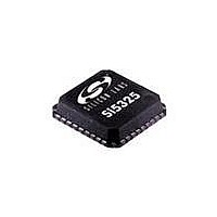
SI5325/26-EVB Silicon Laboratories Inc, SI5325/26-EVB Datasheet - Page 12

SI5325/26-EVB
Manufacturer Part Number
SI5325/26-EVB
Description
BOARD EVAL FOR SI5325/26
Manufacturer
Silicon Laboratories Inc
Specifications of SI5325/26-EVB
Main Purpose
Timing, Clock Generator
Utilized Ic / Part
SI5325, SI5326
Processor To Be Evaluated
Si5325 and Si5326
Lead Free Status / RoHS Status
Lead free / RoHS Compliant
Secondary Attributes
-
Embedded
-
Primary Attributes
-
Lead Free Status / Rohs Status
Lead free / RoHS Compliant
Si5326
12
Table 4. AC Specifications (Continued)
(V
Output Rise/Fall
(20–80%) @
212.5 MHz output
Output Duty Cycle
Uncertainty @
622.08 MHz
LVCMOS Input Pins
Minimum Reset Pulse
Width
Reset to Microproces-
sor Access Ready
Input Capacitance
LVCMOS Output Pins
Rise/Fall Times
LOSn Trigger Window
Time to Clear LOL
after LOS Cleared
Device Skew
Output Clock Skew
Phase Change due to
Temperature Variation
DD
= 1.8 ± 5%, 2.5 ±10%, or 3.3 V ±10%, T
Parameter
LOS
CKO
Symbol
t
CKO
t
t
CLRLOL
t
RSTMN
READY
t
SKEW
TEMP
C
t
RF
in
TRIG
TRF
DC
CKOUT_ALWAYS_ON = 1
Internal detection of LOSn
Max phase changes from
and CKOUT_m at same
A
Measured at 50% Point
Stable Xa/XB reference
From last CKINn to
CKOUT_m, CKOUTn
of CKOUTn to of
frequency and signal
PHASEOFFSET = 0
= –40 to 85 °C)
Test Condition
(Not for CMOS)
LOS to LOL
CMOS Output
–40 to +85 °C
C
C
SQ_ICAL = 1
See Figure 2
Fold = Fnew
100 Load
Line-to-Line
V
LOAD
LOAD
DD
N3 ≠ 1
format
= 2.97
= 5 pF
= 20pf
Rev. 1.0
Min
—
—
—
—
—
—
—
—
1
Typ
300
25
10
—
—
—
—
—
4.5 x N3
+/-40
Max
100
500
10
—
—
2
3
T
Unit
ms
CKIN
ms
pF
ns
ps
µs
ns
ps
ps


