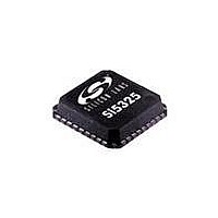
SI5325/26-EVB Silicon Laboratories Inc, SI5325/26-EVB Datasheet - Page 60

SI5325/26-EVB
Manufacturer Part Number
SI5325/26-EVB
Description
BOARD EVAL FOR SI5325/26
Manufacturer
Silicon Laboratories Inc
Specifications of SI5325/26-EVB
Main Purpose
Timing, Clock Generator
Utilized Ic / Part
SI5325, SI5326
Processor To Be Evaluated
Si5325 and Si5326
Lead Free Status / RoHS Status
Lead free / RoHS Compliant
Secondary Attributes
-
Embedded
-
Primary Attributes
-
Lead Free Status / Rohs Status
Lead free / RoHS Compliant
Si5326
60
Note: Internal register names are indicated by underlined italics, e.g., INT_PIN. See Section “5.Register Map”.
Pin #
18
19
20
Pin Name
DEC
LOL
INC
I/O
O
I
I
Signal Level
LVCMOS
LVCMOS
LVCMOS
PLL Loss of Lock Indicator.
This pin functions as the active high PLL loss of lock indicator if the
LOL_PIN register bit is set to 1.
0 = PLL locked
1 = PLL unlocked
If LOL_PIN = 0, this pin will tristate. Active polarity is controlled by
the LOL_POL bit. The PLL lock status will always be reflected in the
LOL_INT read only register bit.
Skew Decrement.
A pulse on this pin decreases the input to output device skew by
1/f
skew adjustment by this method.
Pin control is enabled by setting INCDEC_PIN = 1. If
INCDEC_PIN = 0, this pin is ignored and output skew is controlled
via the CLAT register.
If both INC and DEC are tied high, phase buildout is disabled and
the device maintains a fixed-phase relationship between the
selected input clock and the output clock during an input clock
switch.
See the Si53xx Family Reference Manual for more details.
This pin has a weak pull-down.
Skew Increment.
A pulse on this pin increases the input to output device skew by
1/f
skew adjustment by this method.
Pin control is enabled by setting INCDEC_PIN = 1. If
INCDEC_PIN = 0, this pin is ignored and output skew is controlled
via the CLAT register.
If both INC and DEC are tied high, phase buildout is disabled and
the device maintains a fixed-phase relationship between the
selected input clock and the output clock during an input clock
switch.
See the Si53xx Family Reference Manual for more details.
Note: INC does not increase skew if NI_HS = 4.
This pin has a weak pull-down.
OSC
OSC
(approximately 200 ps). There is no limit on the range of
(approximately 200 ps). There is no limit on the range of
Rev. 1.0
Description


