AT91SAM9M10-G45-EK Atmel, AT91SAM9M10-G45-EK Datasheet - Page 426
AT91SAM9M10-G45-EK
Manufacturer Part Number
AT91SAM9M10-G45-EK
Description
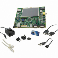
KIT EVAL FOR AT91SAMG45/9M10
Manufacturer
Atmel
Series
AT91SAM Smart ARMr
Type
MCUr
Specifications of AT91SAM9M10-G45-EK
Contents
Board, Cables, Power Supply
Processor To Be Evaluated
AT91SAM9M10
Processor Series
AT91SAM9
Data Bus Width
32 bit
Interface Type
RS-232, Ethernet, USB, JTAG
Operating Supply Voltage
5 V
Silicon Manufacturer
Atmel
Core Architecture
AVR
Kit Contents
Board
Features
Two High Speed USB Hosts, LCD TFT Display
Svhc
No SVHC (15-Dec-2010)
Mcu Supported Families
AT91SAM9M10,
Rohs Compliant
Yes
For Use With/related Products
AT91SAM9M10
Lead Free Status / RoHS Status
Lead free / RoHS Compliant
Available stocks
Company
Part Number
Manufacturer
Quantity
Price
Company:

Part Number:
AT91SAM9M10-G45-EK
Manufacturer:
INFINEON
Quantity:
10 000
Company:
Part Number:
AT91SAM9M10-G45-EK
Manufacturer:
Atmel
Quantity:
135


28.8.9
Name:
Addresses:
Access:
Note:
• CPOL: Clock Polarity
0 = The inactive state value of SPCK is logic level zero.
1 = The inactive state value of SPCK is logic level one.
CPOL is used to determine the inactive state value of the serial clock (SPCK). It is used with NCPHA to produce the
required clock/data relationship between master and slave devices.
• NCPHA: Clock Phase
0 = Data is changed on the leading edge of SPCK and captured on the following edge of SPCK.
1 = Data is captured on the leading edge of SPCK and changed on the following edge of SPCK.
NCPHA determines which edge of SPCK causes data to change and which edge causes data to be captured. NCPHA is
used with CPOL to produce the required clock/data relationship between master and slave devices.
• CSAAT: Chip Select Active After Transfer
0 = The Peripheral Chip Select Line rises as soon as the last transfer is achieved.
1 = The Peripheral Chip Select does not rise after the last transfer is achieved. It remains active until a new transfer is
requested on a different chip select.
• BITS: Bits Per Transfer (See the
The BITS field determines the number of data bits transferred. Reserved values should not be used.
6355B–ATARM–21-Jun-10
31
23
15
7
SPI_CSRx registers must be written even if the user wants to use the defaults. The BITS field will not be updated with the trans-
lated value unless the register is written.
SPI Chip Select Register
30
22
14
SPI_CSR0... SPI_CSR3
0xFFFA4030 (0), 0xFFFA8030 (1)
Read/Write
6
BITS
0000
0001
0010
0011
0100
0101
0110
0111
BITS
(Note:)
29
21
13
5
below the register table;
28
20
12
4
DLYBCT
DLYBS
SCBR
CSAAT
Section 28.8.9 “SPI Chip Select Register” on page
27
19
11
3
Bits Per Transfer
26
18
10
–
2
10
11
12
13
14
15
8
9
AT91SAM9M10
NCPHA
25
17
9
1
CPOL
24
16
8
0
426.)
426
Related parts for AT91SAM9M10-G45-EK
Image
Part Number
Description
Manufacturer
Datasheet
Request
R

Part Number:
Description:
KIT EVAL FOR AT91SAM9M10
Manufacturer:
Atmel
Datasheet:

Part Number:
Description:
IC MCU 16/32BIT ARM9 324TFBGA
Manufacturer:
Atmel
Datasheet:

Part Number:
Description:
At91 Arm Thumb-based Microcontrollers
Manufacturer:
ATMEL Corporation
Datasheet:

Part Number:
Description:
MCU, MPU & DSP Development Tools KICKSTART KIT FOR AT91SAM9 PLUS
Manufacturer:
IAR Systems

Part Number:
Description:
DEV KIT FOR AVR/AVR32
Manufacturer:
Atmel
Datasheet:
Part Number:
Description:
INTERVAL AND WIPE/WASH WIPER CONTROL IC WITH DELAY
Manufacturer:
ATMEL Corporation
Datasheet:
Part Number:
Description:
Low-Voltage Voice-Switched IC for Hands-Free Operation
Manufacturer:
ATMEL Corporation
Datasheet:
Part Number:
Description:
MONOLITHIC INTEGRATED FEATUREPHONE CIRCUIT
Manufacturer:
ATMEL Corporation
Datasheet:
Part Number:
Description:
AM-FM Receiver IC U4255BM-M
Manufacturer:
ATMEL Corporation
Datasheet:
Part Number:
Description:
Monolithic Integrated Feature Phone Circuit
Manufacturer:
ATMEL Corporation
Datasheet:
Part Number:
Description:
Multistandard Video-IF and Quasi Parallel Sound Processing
Manufacturer:
ATMEL Corporation
Datasheet:
Part Number:
Description:
High-performance EE PLD
Manufacturer:
ATMEL Corporation
Datasheet: