EVAL-ADUC7128QSPZ Analog Devices Inc, EVAL-ADUC7128QSPZ Datasheet - Page 18
EVAL-ADUC7128QSPZ
Manufacturer Part Number
EVAL-ADUC7128QSPZ
Description
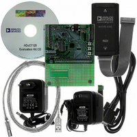
KIT DEV FOR ADUC7128
Manufacturer
Analog Devices Inc
Series
QuickStart™ PLUS Kitr
Type
MCUr
Datasheet
1.EVAL-ADUC7128QSPZ.pdf
(92 pages)
Specifications of EVAL-ADUC7128QSPZ
Contents
Evaluation Board, Power Supply, Cable, Software, Emulator and Documentation
Silicon Manufacturer
Analog Devices
Core Architecture
ARM
Core Sub-architecture
ARM7TDMI
Silicon Core Number
ADuC7128
Rohs Compliant
Yes
Lead Free Status / RoHS Status
Lead free / RoHS Compliant
For Use With/related Products
ADuC7128
Lead Free Status / RoHS Status
Lead free / RoHS Compliant, Lead free / RoHS Compliant


ADuC7128/ADuC7129
Table 11. ADuC7129 Pin Function Descriptions
Pin
No.
1
2
3
4
5
6
7
8
9
10, 73, 74
11
12
13
14
15
16
Mnemonic
ADC4
ADC5
ADC6
ADC7
VDAC
ADC9
ADC10
GND
ADCNEG
AV
ADC12/LD1TX
ADC13/LD2TX
AGND
TMS
TDI/P0.1/BLE
P2.3/AE
DD
REF
OUT
P0.0/BM/CMP
/ADC8
P4.6/SPM10/AD14
P4.7/SPM11/AD15
VDAC
ADC12/LD1TX
ADC13/LD2TX
P0.6/T1/MRST
TDI/P0.1/BLE
OUT
ADCNEG
OUT
GND
P2.3/AE
ADC10
/ADC8
AGND
ADC4
ADC5
ADC6
ADC7
ADC9
AV
/MS0
TMS
REF
DD
10
12
13
14
15
16
17
18
19
11
20
1
2
5
6
7
8
3
4
9
Type
I
I
I
I
I
I
I
S
I
S
I/O
I/O
S
I
I/0
I/O
80 79 78 77 76 75 74 73 72 71 70 69 68 67 66 65 64 63 62 61
21 22 23 24 25 26 27 28 29 30 31 32 33 34 35 36 37 38 39 40
PIN 1
1
Description
Single-Ended or Differential Analog Input 4.
Single-Ended or Differential Analog Input 5.
Single-Ended or Differential Analog Input 6.
Single-Ended or Differential Analog Input 7.
Output from DAC Buffer/Single-Ended or Differential Analog Input 8.
Single-Ended or Differential Analog Input 9.
Single-Ended or Differential Analog Input 10.
Ground Voltage Reference for the ADC. For optimal performance, the analog power supply
should be separated from IOGND and DGND.
Bias Point or Negative Analog Input of the ADC in Pseudo Differential Mode. Must be
connected to the ground of the signal to convert. This bias point must be between
0 V and 1 V.
3.3 V Analog Supply.
Single-Ended or Differential Analog Input 12/DAC Differential Negative Output.
Single-Ended or Differential Analog Input 13/DAC Differential Positive Output.
Analog Ground. Ground reference point for the analog circuitry.
JTAG Test Port Input, Test Mode Select. Debug and download access.
JTAG Test Port Input, Test Data In. Debug and download access/general-purpose input and
output Port 0.1/External Memory BLE.
General-Purpose Input and Output Port 2.3/AE Output.
Figure 11. ADuC7129 Pin Configuration
Rev. 0 | Page 18 of 92
ADuC7129
(Not to Scale)
TOP VIEW
60
59
58
57
56
55
54
53
52
51
50
49
48
47
46
45
44
43
42
41
P1.2/SPM2
P1.3/SPM3
P1.4/SPM4
P1.5/SPM5
P4.1/S2/AD9
P4.0/S1/AD8
IOV
IOGND
P1.6/SPM6
P1.7/SPM7
P2.2/RS
P2.1/WS
P2.7/MS3
P3.7/AD7
P3.6/AD6
DGND
PV
XCLKI
XCLKO
P0.7/SPM8/ECLK/XCLK
DD
DD
Related parts for EVAL-ADUC7128QSPZ
Image
Part Number
Description
Manufacturer
Datasheet
Request
R

Part Number:
Description:
IC, ADJ LDO REG, 1.5V TO 5V 250mA MSOP-8
Manufacturer:
Vishay
Datasheet:

Part Number:
Description:
IC, ADJ LDO REG, 1.5V TO 5V 0.6A 8-TSSOP
Manufacturer:
Vishay
Datasheet:
Part Number:
Description:
IC, ADJ LDO REG, 1.5V TO 5V 250mA MSOP-8
Manufacturer:
Vishay
Datasheet:

Part Number:
Description:
IC ADJ LDO REG 1.5V TO 5V 150mA 5-SOT-23
Manufacturer:
Vishay
Datasheet:

Part Number:
Description:
BOARD EVAL AS1324-AD
Manufacturer:
austriamicrosystems
Datasheet:
Part Number:
Description:
IC, ADJ LDO REG, 1.5V TO 5V 0.6A 8-TSSOP
Manufacturer:
Vishay
Datasheet:

Part Number:
Description:
IC, ADJ LDO REG, 1.5V TO 5V, 0.3A, MSOP8
Manufacturer:
Vishay
Datasheet:
Part Number:
Description:
IC, ADJ LDO REG, 1.5V TO 5V, 0.3A, MSOP8
Manufacturer:
Vishay
Datasheet:
Part Number:
Description:
IC, ADJ LDO REG 1.215V TO 5V 0.3A MSOP-8
Manufacturer:
Vishay
Datasheet:
Part Number:
Description:
IC, ADJ LDO REG 1.215V TO 5V 0.3A MSOP-8
Manufacturer:
Vishay
Datasheet:

Part Number:
Description:
±1.7g Dual-Axis IMEMS Accelerometer Evaluation Board
Manufacturer:
Analog Devices Inc
Datasheet:

Part Number:
Description:
IC MULTIPLIER ANALOG 8-SOIC T/R
Manufacturer:
Analog Devices Inc
Datasheet:

Part Number:
Description:
IC ANALOG MULTIPLIER 8-DIP
Manufacturer:
Analog Devices Inc
Datasheet:
Part Number:
Description:
IC ANALOG MULTIPLIER 8-SOIC
Manufacturer:
Analog Devices Inc
Datasheet:
Part Number:
Description:
IC ANALOG MULTIPLIER 8-DIP
Manufacturer:
Analog Devices Inc
Datasheet: