EVAL-ADUC7128QSPZ Analog Devices Inc, EVAL-ADUC7128QSPZ Datasheet - Page 84
EVAL-ADUC7128QSPZ
Manufacturer Part Number
EVAL-ADUC7128QSPZ
Description
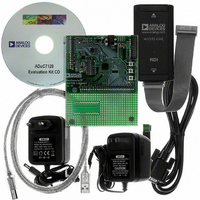
KIT DEV FOR ADUC7128
Manufacturer
Analog Devices Inc
Series
QuickStart™ PLUS Kitr
Type
MCUr
Datasheet
1.EVAL-ADUC7128QSPZ.pdf
(92 pages)
Specifications of EVAL-ADUC7128QSPZ
Contents
Evaluation Board, Power Supply, Cable, Software, Emulator and Documentation
Silicon Manufacturer
Analog Devices
Core Architecture
ARM
Core Sub-architecture
ARM7TDMI
Silicon Core Number
ADuC7128
Rohs Compliant
Yes
Lead Free Status / RoHS Status
Lead free / RoHS Compliant
For Use With/related Products
ADuC7128
Lead Free Status / RoHS Status
Lead free / RoHS Compliant, Lead free / RoHS Compliant


ADuC7128/ADuC7129
The XMxPAR are registers that define the protocol used for accessing the external memory for each memory region.
Table 121. XMxPAR MMR Bit Designations
Bit
15
14:12
11
10
9
8
7:4
3:0
TIMING DIAGRAMS
Figure 62 through Figure 65 show the timing for a read cycle (see Figure 62), a read cycle with address hold and bus turn cycles (see
Figure 63), a write cycle with address hold and write hold cycles (see Figure 64), and a write cycle with wait states (see Figure 65).
Description
Enable Byte Write Strobe. This bit is only used for two,
8-bit memory sharing the same memory region.
Number of Wait States on the Address Latch Enable Strobe.
Reserved.
Extra Address Hold Time.
Extra Bus Transition Time on Read.
Extra Bus Transition Time on Write.
Number of Write Wait States. Select the number of wait states added to the length of the WS pulse. 0x0 is 1 clock cycle; 0xF is 16 clock
cycles (default value).
Number of Read Wait States. Select the number of wait states added to the length of the RS pulse. 0x0 is 1 clock cycle; 0xF is 16 clock
cycles (default value).
Set by user to gate the AD0 output with the WS output. This allows byte write capability without using BHE and BLE signals.
Set by the user to disable extra bus transition time.
Cleared by the user to enable one extra clock before and after the read select (RS).
Set by the user to disable extra bus transition time.
Cleared by the user to enable one extra clock before and after the write select (WS).
Cleared by user to use BHE and BLE signals.
Set by the user to disable extra hold time.
Cleared by the user to enable one clock cycle of hold on the address in read and write.
AD16:0
HCLK
MSx
AE
RS
ADDRESS
Figure 62. External Memory Read Cycle
Rev. 0 | Page 84 of 92
DATA
Related parts for EVAL-ADUC7128QSPZ
Image
Part Number
Description
Manufacturer
Datasheet
Request
R

Part Number:
Description:
IC, ADJ LDO REG, 1.5V TO 5V 250mA MSOP-8
Manufacturer:
Vishay
Datasheet:

Part Number:
Description:
IC, ADJ LDO REG, 1.5V TO 5V 0.6A 8-TSSOP
Manufacturer:
Vishay
Datasheet:
Part Number:
Description:
IC, ADJ LDO REG, 1.5V TO 5V 250mA MSOP-8
Manufacturer:
Vishay
Datasheet:

Part Number:
Description:
IC ADJ LDO REG 1.5V TO 5V 150mA 5-SOT-23
Manufacturer:
Vishay
Datasheet:

Part Number:
Description:
BOARD EVAL AS1324-AD
Manufacturer:
austriamicrosystems
Datasheet:
Part Number:
Description:
IC, ADJ LDO REG, 1.5V TO 5V 0.6A 8-TSSOP
Manufacturer:
Vishay
Datasheet:

Part Number:
Description:
IC, ADJ LDO REG, 1.5V TO 5V, 0.3A, MSOP8
Manufacturer:
Vishay
Datasheet:
Part Number:
Description:
IC, ADJ LDO REG, 1.5V TO 5V, 0.3A, MSOP8
Manufacturer:
Vishay
Datasheet:
Part Number:
Description:
IC, ADJ LDO REG 1.215V TO 5V 0.3A MSOP-8
Manufacturer:
Vishay
Datasheet:
Part Number:
Description:
IC, ADJ LDO REG 1.215V TO 5V 0.3A MSOP-8
Manufacturer:
Vishay
Datasheet:

Part Number:
Description:
±1.7g Dual-Axis IMEMS Accelerometer Evaluation Board
Manufacturer:
Analog Devices Inc
Datasheet:

Part Number:
Description:
IC MULTIPLIER ANALOG 8-SOIC T/R
Manufacturer:
Analog Devices Inc
Datasheet:

Part Number:
Description:
IC ANALOG MULTIPLIER 8-DIP
Manufacturer:
Analog Devices Inc
Datasheet:
Part Number:
Description:
IC ANALOG MULTIPLIER 8-SOIC
Manufacturer:
Analog Devices Inc
Datasheet:
Part Number:
Description:
IC ANALOG MULTIPLIER 8-DIP
Manufacturer:
Analog Devices Inc
Datasheet: