EVAL-ADUC7128QSPZ Analog Devices Inc, EVAL-ADUC7128QSPZ Datasheet - Page 39
EVAL-ADUC7128QSPZ
Manufacturer Part Number
EVAL-ADUC7128QSPZ
Description
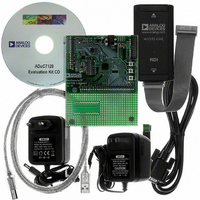
KIT DEV FOR ADUC7128
Manufacturer
Analog Devices Inc
Series
QuickStart™ PLUS Kitr
Type
MCUr
Datasheet
1.EVAL-ADUC7128QSPZ.pdf
(92 pages)
Specifications of EVAL-ADUC7128QSPZ
Contents
Evaluation Board, Power Supply, Cable, Software, Emulator and Documentation
Silicon Manufacturer
Analog Devices
Core Architecture
ARM
Core Sub-architecture
ARM7TDMI
Silicon Core Number
ADuC7128
Rohs Compliant
Yes
Lead Free Status / RoHS Status
Lead free / RoHS Compliant
For Use With/related Products
ADuC7128
Lead Free Status / RoHS Status
Lead free / RoHS Compliant, Lead free / RoHS Compliant


NONVOLATILE FLASH/EE MEMORY
FLASH/EE MEMORY OVERVIEW
The ADuC7128/ADuC7129 incorporate Flash/EE memory
technology on-chip to provide the user with nonvolatile, in-
circuit reprogrammable memory space.
Like EEPROM, Flash memory can be programmed in-system
at a byte level, although it must first be erased. The erase is
performed in page blocks. As a result, Flash memory is often,
and more correctly, referred to as Flash/EE memory.
Overall, Flash/EE memory represents a step closer to the ideal
memory device that includes nonvolatility, in-circuit
programmability, high density, and low cost. Incorporated in
the ADuC7128/ADuC7129, Flash/EE memory technology
allows the user to update program code space in-circuit,
without the need to replace one-time programmable (OTP)
devices at remote operating nodes.
FLASH/EE MEMORY
The ADuC7128/ADuC7129 contain two 64 kB arrays of
Flash/EE memory. In the first block, the lower 62 kB are
available to the user and the upper 2 kB of this Flash/EE
program memory array contain permanently embedded
firmware, allowing in-circuit serial download. The 2 kB of
embedded firmware also contain a power-on configuration
routine that downloads factory calibrated coefficients to the
various calibrated peripherals, such as band gap references.
This 2 kB embedded firmware is hidden from user code. It is not
possible for the user to read, write, or erase this page. In the second
block, all 64 kB of Flash/EE memory are available to the user.
The 126 kB of Flash/EE memory can be programmed in-circuit,
using the serial download mode or the JTAG mode provided.
Flash/EE Memory Reliability
The Flash/EE memory arrays on the parts are fully qualified for
two key Flash/EE memory characteristics: Flash/EE memory
cycling endurance and Flash/EE memory data retention.
Endurance quantifies the ability of the Flash/EE memory to be
cycled through many program, read, and erase cycles. A single
endurance cycle is composed of four independent, sequential
events, defined as
1.
2.
3.
4.
In reliability qualification, every half word (16-bit wide)
location of the three pages (top, middle, and bottom) in
the Flash/EE memory is cycled 10,000 times from 0x0000
to 0xFFFF.
Initial page erase sequence
Read/verify, sequence a single Flash/EE location
Byte program sequence memory
Second read/verify sequence endurance cycle
Rev. 0 | Page 39 of 92
As indicated in Table 1 of the Specifications section, the
Flash/EE memory endurance qualification is carried out in
accordance with JEDEC Retention Lifetime Specification A117
over the industrial temperature range of –40° to +125°C. The
results allow the specification of a minimum endurance figure
over a supply temperature of 10,000 cycles.
Retention quantifies the ability of the Flash/EE memory to
retain its programmed data over time. Again, the parts are
qualified in accordance with the formal JEDEC Retention
Lifetime Specification (A117) at a specific junction temperature
(T
Flash/EE memory is cycled to its specified endurance limit,
described previously, before data retention is characterized.
This means that the Flash/EE memory is guaranteed to retain
its data for its fully specified retention lifetime every time the
Flash/EE memory is reprogrammed. Note, too, that retention
lifetime, based on an activation energy of 0.6 eV, derates with
T
Serial Downloading (In-Circuit Programming)
The ADuC7128/ADuC7129 facilitate code download via the
standard UART serial port. The ADuC7128/ADuC7129 enter
serial download mode after a reset or power cycle if the BM pin
is pulled low through an external 1 kΩ resistor. Once in serial
download mode, the user can download code to the full 126 kB
of Flash/EE memory while the device is in-circuit in its target appli-
cation hardware. A PC serial download executable is provided as
part of the development system for serial downloads via the UART.
For additional information, an application note is available at
www.analog.com/microconverter
serial downloads via the UART.
JTAG Access
The JTAG protocol uses the on-chip JTAG interface to
facilitate code download and debug.
J
, as shown in Figure 44.
J
= 85°C). As part of this qualification procedure, the
600
450
300
150
0
30
Figure 44. Flash/EE Memory Data Retention
40
JUNCTION TEMPERATURE (°C)
55
70
ADuC7128/ADuC7129
85
describing the protocol for
100
125
135
150
Related parts for EVAL-ADUC7128QSPZ
Image
Part Number
Description
Manufacturer
Datasheet
Request
R

Part Number:
Description:
IC, ADJ LDO REG, 1.5V TO 5V 250mA MSOP-8
Manufacturer:
Vishay
Datasheet:

Part Number:
Description:
IC, ADJ LDO REG, 1.5V TO 5V 0.6A 8-TSSOP
Manufacturer:
Vishay
Datasheet:
Part Number:
Description:
IC, ADJ LDO REG, 1.5V TO 5V 250mA MSOP-8
Manufacturer:
Vishay
Datasheet:

Part Number:
Description:
IC ADJ LDO REG 1.5V TO 5V 150mA 5-SOT-23
Manufacturer:
Vishay
Datasheet:

Part Number:
Description:
BOARD EVAL AS1324-AD
Manufacturer:
austriamicrosystems
Datasheet:
Part Number:
Description:
IC, ADJ LDO REG, 1.5V TO 5V 0.6A 8-TSSOP
Manufacturer:
Vishay
Datasheet:

Part Number:
Description:
IC, ADJ LDO REG, 1.5V TO 5V, 0.3A, MSOP8
Manufacturer:
Vishay
Datasheet:
Part Number:
Description:
IC, ADJ LDO REG, 1.5V TO 5V, 0.3A, MSOP8
Manufacturer:
Vishay
Datasheet:
Part Number:
Description:
IC, ADJ LDO REG 1.215V TO 5V 0.3A MSOP-8
Manufacturer:
Vishay
Datasheet:
Part Number:
Description:
IC, ADJ LDO REG 1.215V TO 5V 0.3A MSOP-8
Manufacturer:
Vishay
Datasheet:

Part Number:
Description:
±1.7g Dual-Axis IMEMS Accelerometer Evaluation Board
Manufacturer:
Analog Devices Inc
Datasheet:

Part Number:
Description:
IC MULTIPLIER ANALOG 8-SOIC T/R
Manufacturer:
Analog Devices Inc
Datasheet:

Part Number:
Description:
IC ANALOG MULTIPLIER 8-DIP
Manufacturer:
Analog Devices Inc
Datasheet:
Part Number:
Description:
IC ANALOG MULTIPLIER 8-SOIC
Manufacturer:
Analog Devices Inc
Datasheet:
Part Number:
Description:
IC ANALOG MULTIPLIER 8-DIP
Manufacturer:
Analog Devices Inc
Datasheet: