EVAL-ADUC7128QSPZ Analog Devices Inc, EVAL-ADUC7128QSPZ Datasheet - Page 5
EVAL-ADUC7128QSPZ
Manufacturer Part Number
EVAL-ADUC7128QSPZ
Description
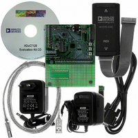
KIT DEV FOR ADUC7128
Manufacturer
Analog Devices Inc
Series
QuickStart™ PLUS Kitr
Type
MCUr
Datasheet
1.EVAL-ADUC7128QSPZ.pdf
(92 pages)
Specifications of EVAL-ADUC7128QSPZ
Contents
Evaluation Board, Power Supply, Cable, Software, Emulator and Documentation
Silicon Manufacturer
Analog Devices
Core Architecture
ARM
Core Sub-architecture
ARM7TDMI
Silicon Core Number
ADuC7128
Rohs Compliant
Yes
Lead Free Status / RoHS Status
Lead free / RoHS Compliant
For Use With/related Products
ADuC7128
Lead Free Status / RoHS Status
Lead free / RoHS Compliant, Lead free / RoHS Compliant


Parameter
COMMON MODE
DIFFERENTIAL INPUT IMPEDANCE
COMPARATOR
TEMPERATURE SENSOR
POWER SUPPLY MONITOR (PSM)
IOV
GLITCH IMMUNITY ON RST PIN
WATCHDOG TIMER (WDT)
FLASH/EE MEMORY
DIGITAL INPUTS
Input Offset Voltage
Input Bias Current
Input Voltage Range
Input Capacitance
Hysteresis
Response Time
Voltage Output at 25°C
Voltage Temperature Coefficient
Accuracy
Power Supply Trip Point Accuracy
Timeout Period
Endurance
Data Retention
Logic 0 Input Current (Leakage
Input Capacitance
Line Driver Output
AC Mode
DC Mode
Leakage Current LD1TX, LD2TX
Logic 1 Input Current (Leakage
DD
Line Driver Tx Power-Up Time
Relative Accuracy
Differential Nonlinearity, +VE
Differential Nonlinearity, −VE
Offset Error
Gain Error
Voltage Output Settling Time
Total Harmonic Distortion
Output Voltage Swing
Short-Circuit Current
Current)
Current)
Trip Point Selection
to 0.1%
3, 5
7, 8
3
Min
11
AGND
2
0
10,000
20
Typ
±2
0.35
−0.15
±1.768
1.65
1.5
13
±50
±15
7
1
780
−1.3
±3
3.07
±2.5
50
±0.2
−40
−80
15
−52
1
2.79
Rev. 0 | Page 5 of 92
Max
−190
+150
5
7
20
AV
15
512
±1
−65
+125
DD
− 1.2 V
Unit
LSB
LSB
LSB
mV
mV
μs
dB
V rms
V
V
kΩ
μA
mA
μs
mV
μA
pF
mV
μs
mV
mV/°C
°C
V
V
%
μs
ms
sec
Cycles
Years
μA
μA
μA
pF
Test Conditions/Comments
As measured into a range of specified loads
(see Figure 2) at LD1TX and LD2TX, unless
otherwise noted
PLM operating at 691.2 kHz
Each output has a common mode of 0.5 V × AV
and swings 0.5 V × V
V
Each output has a common mode of 0.5 V × V
and swings 0.6 V × V
V
Line driver buffer disabled
Line driver buffer disabled
No protection diodes, max allowable current
Hysteresis can be turned on or off via the
CMPHYST bit in the CMPCON register
Response time can be modified via the CMPRES
bits in the CMPCON register
Two selectable trip points
Of the selected nominal trip point voltage
T
All digital inputs, including XCLKI and XCLKO
V
V
V
J
REF
REF
INH
INL
INL
= 85°C
= 0 V, except TDI
= 0 V, TDI Only
is the internal 2.5 V reference
is the internal 2.5 V reference
= V
DD
or V
ADuC7128/ADuC7129
INH
= 5 V
REF
REF
above and below this;
above and below this;
DD
REF
Related parts for EVAL-ADUC7128QSPZ
Image
Part Number
Description
Manufacturer
Datasheet
Request
R

Part Number:
Description:
IC, ADJ LDO REG, 1.5V TO 5V 250mA MSOP-8
Manufacturer:
Vishay
Datasheet:

Part Number:
Description:
IC, ADJ LDO REG, 1.5V TO 5V 0.6A 8-TSSOP
Manufacturer:
Vishay
Datasheet:
Part Number:
Description:
IC, ADJ LDO REG, 1.5V TO 5V 250mA MSOP-8
Manufacturer:
Vishay
Datasheet:

Part Number:
Description:
IC ADJ LDO REG 1.5V TO 5V 150mA 5-SOT-23
Manufacturer:
Vishay
Datasheet:

Part Number:
Description:
BOARD EVAL AS1324-AD
Manufacturer:
austriamicrosystems
Datasheet:
Part Number:
Description:
IC, ADJ LDO REG, 1.5V TO 5V 0.6A 8-TSSOP
Manufacturer:
Vishay
Datasheet:

Part Number:
Description:
IC, ADJ LDO REG, 1.5V TO 5V, 0.3A, MSOP8
Manufacturer:
Vishay
Datasheet:
Part Number:
Description:
IC, ADJ LDO REG, 1.5V TO 5V, 0.3A, MSOP8
Manufacturer:
Vishay
Datasheet:
Part Number:
Description:
IC, ADJ LDO REG 1.215V TO 5V 0.3A MSOP-8
Manufacturer:
Vishay
Datasheet:
Part Number:
Description:
IC, ADJ LDO REG 1.215V TO 5V 0.3A MSOP-8
Manufacturer:
Vishay
Datasheet:

Part Number:
Description:
±1.7g Dual-Axis IMEMS Accelerometer Evaluation Board
Manufacturer:
Analog Devices Inc
Datasheet:

Part Number:
Description:
IC MULTIPLIER ANALOG 8-SOIC T/R
Manufacturer:
Analog Devices Inc
Datasheet:

Part Number:
Description:
IC ANALOG MULTIPLIER 8-DIP
Manufacturer:
Analog Devices Inc
Datasheet:
Part Number:
Description:
IC ANALOG MULTIPLIER 8-SOIC
Manufacturer:
Analog Devices Inc
Datasheet:
Part Number:
Description:
IC ANALOG MULTIPLIER 8-DIP
Manufacturer:
Analog Devices Inc
Datasheet: