EVAL-ADUC7128QSPZ Analog Devices Inc, EVAL-ADUC7128QSPZ Datasheet - Page 25
EVAL-ADUC7128QSPZ
Manufacturer Part Number
EVAL-ADUC7128QSPZ
Description
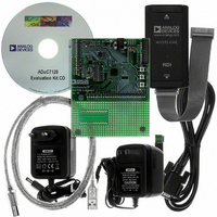
KIT DEV FOR ADUC7128
Manufacturer
Analog Devices Inc
Series
QuickStart™ PLUS Kitr
Type
MCUr
Datasheet
1.EVAL-ADUC7128QSPZ.pdf
(92 pages)
Specifications of EVAL-ADUC7128QSPZ
Contents
Evaluation Board, Power Supply, Cable, Software, Emulator and Documentation
Silicon Manufacturer
Analog Devices
Core Architecture
ARM
Core Sub-architecture
ARM7TDMI
Silicon Core Number
ADuC7128
Rohs Compliant
Yes
Lead Free Status / RoHS Status
Lead free / RoHS Compliant
For Use With/related Products
ADuC7128
Lead Free Status / RoHS Status
Lead free / RoHS Compliant, Lead free / RoHS Compliant


OVERVIEW OF THE ARM7TDMI CORE
The ARM7 core is a 32-bit reduced instruction set computer
(RISC). It uses a single 32-bit bus for instruction and data. The
length of the data can be 8 bits, 16 bits, or 32 bits. The length of
the instruction word is 32 bits.
The ARM7TDMI is an ARM7 core with the following four
additional features:
•
•
•
•
THUMB MODE (T)
An ARM® instruction is 32-bits long. The ARM7TDMI processor
supports a second instruction set that has been compressed into
16-bits, called the Thumb instruction set. Faster execution from
16-bit memory and greater code density can usually be achieved
by using the Thumb instruction set instead of the ARM instruction
set, which makes the ARM7TDMI core particularly suitable for
embedded applications.
However, the Thumb mode has two limitations:
•
•
See the ARM7TDMI user guide for details on the core
architecture, the programming model, and both the ARM
and Thumb instruction sets.
LONG MULTIPLY (M)
The ARM7TDMI instruction set includes four extra instruc-
tions that perform 32-bit by 32-bit multiplication with 64-bit
result, and 32-bit by 32-bit multiplication-accumulation (MAC)
with 64-bit result. This result is achieved in fewer cycles than
required on a standard ARM7 core.
EMBEDDEDICE (I)
EmbeddedICE provides integrated on-chip support for the core.
The EmbeddedICE module contains the breakpoint and watch-
point registers that allow code to be halted for debugging purposes.
These registers are controlled through the JTAG test port.
When a breakpoint or watchpoint is encountered, the processor
halts and enters debug state. Once in a debug state, the processor
registers can be inspected, as well as the Flash/EE, the SRAM,
and the memory mapped registers.
T, support for the Thumb® (16-bit) instruction set
D, support for debug
M, support for long multiplications
I, includes the embedded ICE module to support
embedded system debugging
Thumb code typically requires more instructions for the
same job. As a result, ARM code is usually best for
maximizing the performance of the time-critical code.
The Thumb instruction set does not include some of the
instructions needed for exception handling, which auto-
matically switches the core to ARM code for exception
handling.
Rev. 0 | Page 25 of 92
EXCEPTIONS
ARM supports five types of exceptions and a privileged processing
mode for each type. The five types of exceptions are
•
•
•
•
•
Typically, the programmer defines interrupt as IRQ, but for
higher priority interrupt, that is, faster response time, the
programmer can define interrupt as FIQ.
ARM REGISTERS
ARM7TDMI has a total of 37 registers: 31 general-purpose
registers and six status registers. Each operating mode has
dedicated banked registers.
When writing user-level programs, 15 general-purpose, 32-bit
registers (R0 to R14), the program counter (R15), and the current
program status register (CPSR) are usable. The remaining registers
are used only for system-level programming and exception
handling.
When an exception occurs, some of the standard registers are
replaced with registers specific to the exception mode. All
exception modes have replacement banked registers for the
stack pointer (R13) and the link register (R14), as represented
in Figure 28. The fast interrupt mode has more registers (R8 to
R12) for fast interrupt processing. Interrupt processing can begin
without the need to save or restore these registers and, thus,
saves critical time in the interrupt handling process.
More information relative to the programmer’s model and the
ARM7TDMI core architecture can be found in the following
ARM7TDMI technical and ARM architecture manuals available
directly from ARM Ltd.:
•
•
Normal interrupt or IRQ. This is provided to service
general-purpose interrupt handling of internal and
external events.
Fast interrupt or FIQ. This is provided to service data
transfer or communication channel with low latency.
FIQ has priority over IRQ.
Memory abort.
Attempted execution of an undefined instruction.
Software interrupt instruction (SWI). This can be used to
make a call to an operating system.
DDI0029G, ARM7TDMI Technical Reference Manual
DDI-0100, ARM Architecture Reference Manual
ADuC7128/ADuC7129
Related parts for EVAL-ADUC7128QSPZ
Image
Part Number
Description
Manufacturer
Datasheet
Request
R

Part Number:
Description:
IC, ADJ LDO REG, 1.5V TO 5V 250mA MSOP-8
Manufacturer:
Vishay
Datasheet:

Part Number:
Description:
IC, ADJ LDO REG, 1.5V TO 5V 0.6A 8-TSSOP
Manufacturer:
Vishay
Datasheet:
Part Number:
Description:
IC, ADJ LDO REG, 1.5V TO 5V 250mA MSOP-8
Manufacturer:
Vishay
Datasheet:

Part Number:
Description:
IC ADJ LDO REG 1.5V TO 5V 150mA 5-SOT-23
Manufacturer:
Vishay
Datasheet:

Part Number:
Description:
BOARD EVAL AS1324-AD
Manufacturer:
austriamicrosystems
Datasheet:
Part Number:
Description:
IC, ADJ LDO REG, 1.5V TO 5V 0.6A 8-TSSOP
Manufacturer:
Vishay
Datasheet:

Part Number:
Description:
IC, ADJ LDO REG, 1.5V TO 5V, 0.3A, MSOP8
Manufacturer:
Vishay
Datasheet:
Part Number:
Description:
IC, ADJ LDO REG, 1.5V TO 5V, 0.3A, MSOP8
Manufacturer:
Vishay
Datasheet:
Part Number:
Description:
IC, ADJ LDO REG 1.215V TO 5V 0.3A MSOP-8
Manufacturer:
Vishay
Datasheet:
Part Number:
Description:
IC, ADJ LDO REG 1.215V TO 5V 0.3A MSOP-8
Manufacturer:
Vishay
Datasheet:

Part Number:
Description:
±1.7g Dual-Axis IMEMS Accelerometer Evaluation Board
Manufacturer:
Analog Devices Inc
Datasheet:

Part Number:
Description:
IC MULTIPLIER ANALOG 8-SOIC T/R
Manufacturer:
Analog Devices Inc
Datasheet:

Part Number:
Description:
IC ANALOG MULTIPLIER 8-DIP
Manufacturer:
Analog Devices Inc
Datasheet:
Part Number:
Description:
IC ANALOG MULTIPLIER 8-SOIC
Manufacturer:
Analog Devices Inc
Datasheet:
Part Number:
Description:
IC ANALOG MULTIPLIER 8-DIP
Manufacturer:
Analog Devices Inc
Datasheet: