EVAL-ADUC7026QSPZ Analog Devices Inc, EVAL-ADUC7026QSPZ Datasheet - Page 19
EVAL-ADUC7026QSPZ
Manufacturer Part Number
EVAL-ADUC7026QSPZ
Description
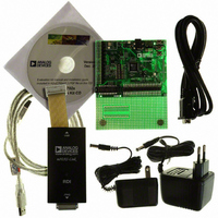
KIT DEV ADUC7026/7027 QUICK PLUS
Manufacturer
Analog Devices Inc
Series
QuickStart™ PLUS Kitr
Type
MCUr
Specifications of EVAL-ADUC7026QSPZ
Contents
Evaluation Board, Power Supply, Cable, Software, Emulator and Documentation
Silicon Manufacturer
Analog Devices
Core Architecture
ARM
Core Sub-architecture
ARM7TDMI
Silicon Core Number
ADuC7026
Rohs Compliant
Yes
Lead Free Status / RoHS Status
Lead free / RoHS Compliant
For Use With/related Products
ADuC7026
Lead Free Status / Rohs Status
Compliant
Available stocks
Company
Part Number
Manufacturer
Quantity
Price
Company:

Part Number:
EVAL-ADUC7026QSPZ
Manufacturer:
Analog Devices Inc
Quantity:
135


7019/7020
11
12
13
14
15
16
17
18
19
20
21
22
23
24
25
26
27
28
29
30
31
32
33
34
35
36
37
Pin No.
7021
11
12
13
14
15
16
17
18
19
20
21
22
23
24
25
26
27
28
29
30
31
32
33
‒
34
35
36
7022
10
11
12
13
14
15
16
17
18
19
20
21
22
23
24
25
26
27
28
29
30
31
32
‒
33
34
35
P0.6/T1/MRST/PLAO[3]
TCK
TDO
IOGND
IOV
LV
DGND
P0.3/TRST/ADC
RST
IRQ0/P0.4/PWM
IRQ1/P0.5/ADC
P2.0/SPM9/PLAO[5]/CONV
P0.7/ECLK/XCLK/SPM8/PLAO[4]
XCLKO
XCLKI
P1.7/SPM7/PLAO[0]
P1.6/SPM6/PLAI[6]
P1.5/SPM5/PLAI[5]/IRQ3
P1.4/SPM4/PLAI[4]/IRQ2
P1.3/SPM3/PLAI[3]
P1.2/SPM2/PLAI[2]
P1.1/SPM1/PLAI[1]
P1.0/T1/SPM0/PLAI[0]
P4.2/PLAO[10]
V
AGND
AV
Mnemonic
REF
DD
DD
DD
BUSY
BUSY
TRIP
/PLAO[2]
/PLAO[1]
START
Rev. B | Page 19 of 92
Description
Multifunction Pin. Driven low after reset. General-Purpose Output Port 0.6/
Timer1 Input/Power-On Reset Output/Programmable Logic Array Output
Element 3.
Test Clock, JTAG Test Port Input. Debug and download access.
Test Data Out, JTAG Test Port Output. Debug and download access.
Ground for GPIO. Typically connected to DGND.
3.3 V Supply for GPIO and Input of the On-Chip Voltage Regulator.
2.6 V Output of the On-Chip Voltage Regulator. This output must be
connected to a 0.47 μF capacitor to DGND only.
Ground for Core Logic.
General-Purpose Input and Output Port 0.3/Test Reset, JTAG Test Port Input/
ADC
Reset Input, Active Low.
Multifunction I/O Pin. External Interrupt Request 0, Active High/General-
Purpose Input and Output Port 0.4/PWM Trip External Input/Programmable
Logic Array Output Element 1.
Multifunction I/O Pin. External Interrupt Request 1, Active High/General-
Purpose Input and Output Port 0.5/ADC
Logic Array Output Element 2.
Serial Port Multiplexed. General-Purpose Input and Output Port 2.0/UART/
Programmable Logic Array Output Element 5/Start Conversion Input Signal
for ADC.
Serial Port Multiplexed. General-Purpose Input and Output Port 0.7/
Output for External Clock Signal/Input to the Internal Clock Generator
Circuits/UART/ Programmable Logic Array Output Element 4.
Output from the Crystal Oscillator Inverter.
Input to the Crystal Oscillator Inverter and Input to the Internal Clock
Generator Circuits.
Serial Port Multiplexed. General-Purpose Input and Output Port 1.7/UART,
SPI/Programmable Logic Array Output Element 0.
Serial Port Multiplexed. General-Purpose Input and Output Port 1.6/UART,
SPI/Programmable Logic Array Input Element 6.
Serial Port Multiplexed. General-Purpose Input and Output Port 1.5/UART,
SPI/Programmable Logic Array Input Element 5/External Interrupt
Request 3, Active High.
Serial Port Multiplexed. General-Purpose Input and Output Port 1.4/UART,
SPI/Programmable Logic Array Input Element 4/External Interrupt
Request 2, Active High.
Serial Port Multiplexed. General-Purpose Input and Output Port 1.3/UART,
I2C1/Programmable Logic Array Input Element 3.
Serial Port Multiplexed. General-Purpose Input and Output Port 1.2/UART,
I2C1/Programmable Logic Array Input Element 2.
Serial Port Multiplexed. General-Purpose Input and Output Port 1.1/UART,
I2C0/Programmable Logic Array Input Element 1.
Serial Port Multiplexed. General-Purpose Input and Output Port 1.0/
Timer1 Input/ UART, I2C0/Programmable Logic Array Input Element 0.
General-Purpose Input and Output Port 4.2/Programmable Logic Array
Output Element 10.
2.5 V Internal Voltage Reference. Must be connected to a 0.47 μF capacitor
when using the internal reference.
Analog Ground. Ground reference point for the analog circuitry.
3.3 V Analog Power.
BUSY
Signal Output.
ADuC7019/20/21/22/24/25/26/27/28
BUSY
Signal Output/Programmable
Related parts for EVAL-ADUC7026QSPZ
Image
Part Number
Description
Manufacturer
Datasheet
Request
R

Part Number:
Description:
IC, ADJ LDO REG, 1.5V TO 5V 250mA MSOP-8
Manufacturer:
Vishay
Datasheet:

Part Number:
Description:
IC, ADJ LDO REG, 1.5V TO 5V 0.6A 8-TSSOP
Manufacturer:
Vishay
Datasheet:
Part Number:
Description:
IC, ADJ LDO REG, 1.5V TO 5V 250mA MSOP-8
Manufacturer:
Vishay
Datasheet:

Part Number:
Description:
IC ADJ LDO REG 1.5V TO 5V 150mA 5-SOT-23
Manufacturer:
Vishay
Datasheet:

Part Number:
Description:
BOARD EVAL AS1324-AD
Manufacturer:
austriamicrosystems
Datasheet:
Part Number:
Description:
IC, ADJ LDO REG, 1.5V TO 5V 0.6A 8-TSSOP
Manufacturer:
Vishay
Datasheet:

Part Number:
Description:
IC, ADJ LDO REG, 1.5V TO 5V, 0.3A, MSOP8
Manufacturer:
Vishay
Datasheet:
Part Number:
Description:
IC, ADJ LDO REG, 1.5V TO 5V, 0.3A, MSOP8
Manufacturer:
Vishay
Datasheet:
Part Number:
Description:
IC, ADJ LDO REG 1.215V TO 5V 0.3A MSOP-8
Manufacturer:
Vishay
Datasheet:
Part Number:
Description:
IC, ADJ LDO REG 1.215V TO 5V 0.3A MSOP-8
Manufacturer:
Vishay
Datasheet:

Part Number:
Description:
±1.7g Dual-Axis IMEMS Accelerometer Evaluation Board
Manufacturer:
Analog Devices Inc
Datasheet:

Part Number:
Description:
IC MULTIPLIER ANALOG 8-SOIC T/R
Manufacturer:
Analog Devices Inc
Datasheet:

Part Number:
Description:
IC ANALOG MULTIPLIER 8-DIP
Manufacturer:
Analog Devices Inc
Datasheet:
Part Number:
Description:
IC ANALOG MULTIPLIER 8-SOIC
Manufacturer:
Analog Devices Inc
Datasheet:
Part Number:
Description:
IC ANALOG MULTIPLIER 8-DIP
Manufacturer:
Analog Devices Inc
Datasheet: