EVAL-ADUC7026QSPZ Analog Devices Inc, EVAL-ADUC7026QSPZ Datasheet - Page 49
EVAL-ADUC7026QSPZ
Manufacturer Part Number
EVAL-ADUC7026QSPZ
Description
KIT DEV ADUC7026/7027 QUICK PLUS
Manufacturer
Analog Devices Inc
Series
QuickStart™ PLUS Kitr
Type
MCUr
Specifications of EVAL-ADUC7026QSPZ
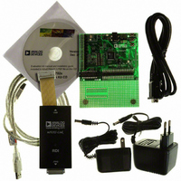
Contents
Evaluation Board, Power Supply, Cable, Software, Emulator and Documentation
Silicon Manufacturer
Analog Devices
Core Architecture
ARM
Core Sub-architecture
ARM7TDMI
Silicon Core Number
ADuC7026
Rohs Compliant
Yes
Lead Free Status / RoHS Status
Lead free / RoHS Compliant
For Use With/related Products
ADuC7026
Lead Free Status / Rohs Status
Compliant
Available stocks
Company
Part Number
Manufacturer
Quantity
Price
Company:

Part Number:
EVAL-ADUC7026QSPZ
Manufacturer:
Analog Devices Inc
Quantity:
135


OTHER ANALOG PERIPHERALS
DAC
The ADuC7019/20/21/22/24/25/26/27/28 incorporate two,
three, or four, 12-bit voltage output DACs on-chip, depending on
the model. Each DAC has a rail-to-rail voltage output buffer
capable of driving 5 kΩ/100 pF.
Each DAC has three selectable ranges: 0 V to V
band gap 2.5 V reference), 0 V to DAC
DAC
The signal range is 0 V to AV
MMRs Interface
Each DAC is independently configurable through a control
register and a data register. These two registers are identical for
the four DACs. Only DAC0CON (see Table 27) and DAC0DAT
(see Table 28) are described in detail in this section.
DACxCON Registers
Name
DAC0CON
DAC1CON
DAC2CON
DAC3CON
Table 27. DAC0CON MMR Bit Designations
Bit
7:6
5
4
3
2
1:0
REF
Value
00
01
10
11
is equivalent to an external reference for the DAC.
Address
0xFFFF0600
0xFFFF0608
0xFFFF0610
0xFFFF0618
Name
DACCLK
DACCLR
Description
Reserved.
DAC Update Rate. Set by user to
update the DAC using Timer1.
Cleared by user to update the DAC
using HCLK (core clock).
DAC Clear Bit. Set by user to enable
normal DAC operation. Cleared by
user to reset data register of the DAC
to 0.
Reserved. This bit should be left at 0.
Reserved. This bit should be left at 0.
DAC Range Bits.
Power-Down Mode. The DAC output
is in tristate.
0 V to DAC
0 V to V
0 V to AV
DD
.
Default Value
0x00
0x00
0x00
0x00
REF
DD
(2.5 V) Range.
REF
REF,
Range.
Range.
and 0 V to AV
REF
(internal
Access
R/W
R/W
R/W
R/W
DD
.
Rev. B | Page 49 of 92
DACxDAT Registers
Name
DAC0DAT
DAC1DAT
DAC2DAT
DAC3DAT
Table 28. DAC0DAT MMR Bit Designations
Bit
31:28
27:16
15:0
Using the DACs
The on-chip DAC architecture consists of a resistor string DAC
followed by an output buffer amplifier. The functional equivalent
is shown in Figure 52.
As illustrated in Figure 52, the reference source for each DAC is
user-selectable in software. It can be either AV
In 0-to-AV
from 0 V to the voltage at the AV
the DAC output transfer function spans from 0 V to the voltage at
the DAC
function spans from 0 V to the internal 2.5 V reference, V
The DAC output buffer amplifier features a true, rail-to-rail
output stage implementation. This means that when unloaded,
each output is capable of swinging to within less than 5 mV of
both AV
(when driving a 5 kΩ resistive load to ground) is guaranteed
through the full transfer function except codes 0 to 100, and, in
0-to-AV
ADuC7019/20/21/22/24/25/26/27/28
DD
DD
REF
and ground. Moreover, the DAC’s linearity specification
DD
mode only, codes 3995 to 4095.
pin. In 0-to-V
DAC
mode, the DAC output transfer function spans
AV
V
Address
0xFFFF0604
0xFFFF060C
0xFFFF0614
0xFFFF061C
REF
REF
DD
Description
Reserved.
12-Bit Data for DAC0.
Reserved.
Figure 52. DAC Structure
REF
R
R
R
R
R
mode, the DAC output transfer
DD
Default Value
0x00000000
0x00000000
0x00000000
0x00000000
pin. In 0-to-DAC
DD
, V
DAC0
REF
REF
, or DAC
mode,
Access
R/W
R/W
R/W
R/W
REF
.
REF
.
Related parts for EVAL-ADUC7026QSPZ
Image
Part Number
Description
Manufacturer
Datasheet
Request
R

Part Number:
Description:
IC, ADJ LDO REG, 1.5V TO 5V 250mA MSOP-8
Manufacturer:
Vishay
Datasheet:

Part Number:
Description:
IC, ADJ LDO REG, 1.5V TO 5V 0.6A 8-TSSOP
Manufacturer:
Vishay
Datasheet:
Part Number:
Description:
IC, ADJ LDO REG, 1.5V TO 5V 250mA MSOP-8
Manufacturer:
Vishay
Datasheet:

Part Number:
Description:
IC ADJ LDO REG 1.5V TO 5V 150mA 5-SOT-23
Manufacturer:
Vishay
Datasheet:

Part Number:
Description:
BOARD EVAL AS1324-AD
Manufacturer:
austriamicrosystems
Datasheet:
Part Number:
Description:
IC, ADJ LDO REG, 1.5V TO 5V 0.6A 8-TSSOP
Manufacturer:
Vishay
Datasheet:

Part Number:
Description:
IC, ADJ LDO REG, 1.5V TO 5V, 0.3A, MSOP8
Manufacturer:
Vishay
Datasheet:
Part Number:
Description:
IC, ADJ LDO REG, 1.5V TO 5V, 0.3A, MSOP8
Manufacturer:
Vishay
Datasheet:
Part Number:
Description:
IC, ADJ LDO REG 1.215V TO 5V 0.3A MSOP-8
Manufacturer:
Vishay
Datasheet:
Part Number:
Description:
IC, ADJ LDO REG 1.215V TO 5V 0.3A MSOP-8
Manufacturer:
Vishay
Datasheet:

Part Number:
Description:
±1.7g Dual-Axis IMEMS Accelerometer Evaluation Board
Manufacturer:
Analog Devices Inc
Datasheet:

Part Number:
Description:
IC MULTIPLIER ANALOG 8-SOIC T/R
Manufacturer:
Analog Devices Inc
Datasheet:

Part Number:
Description:
IC ANALOG MULTIPLIER 8-DIP
Manufacturer:
Analog Devices Inc
Datasheet:
Part Number:
Description:
IC ANALOG MULTIPLIER 8-SOIC
Manufacturer:
Analog Devices Inc
Datasheet:
Part Number:
Description:
IC ANALOG MULTIPLIER 8-DIP
Manufacturer:
Analog Devices Inc
Datasheet: