EVAL-ADUC7026QSPZ Analog Devices Inc, EVAL-ADUC7026QSPZ Datasheet - Page 84
EVAL-ADUC7026QSPZ
Manufacturer Part Number
EVAL-ADUC7026QSPZ
Description
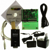
KIT DEV ADUC7026/7027 QUICK PLUS
Manufacturer
Analog Devices Inc
Series
QuickStart™ PLUS Kitr
Type
MCUr
Specifications of EVAL-ADUC7026QSPZ
Contents
Evaluation Board, Power Supply, Cable, Software, Emulator and Documentation
Silicon Manufacturer
Analog Devices
Core Architecture
ARM
Core Sub-architecture
ARM7TDMI
Silicon Core Number
ADuC7026
Rohs Compliant
Yes
Lead Free Status / RoHS Status
Lead free / RoHS Compliant
For Use With/related Products
ADuC7026
Lead Free Status / Rohs Status
Compliant
Available stocks
Company
Part Number
Manufacturer
Quantity
Price
Company:

Part Number:
EVAL-ADUC7026QSPZ
Manufacturer:
Analog Devices Inc
Quantity:
135


ADuC7019/20/21/22/24/25/26/27/28
HARDWARE DESIGN CONSIDERATIONS
POWER SUPPLIES
The ADuC7019/20/21/22/24/25/26/27/28 operational power
supply voltage range is 2.7 V to 3.6 V. Separate analog and
digital power supply pins (AV
AV
present on the system IOV
also operate with split supplies, that is, it can use different
voltage levels for each supply. For example, the system can be
designed to operate with an IOV
the AV
configuration is shown in Figure 74.
As an alternative to providing two separate power supplies, the
user can reduce noise on AV
and/or ferrite bead between AV
AV
shown in Figure 75. With this configuration, other analog circuitry
(such as op amps, voltage reference, and others) can be powered
from the AV
Notice that in both Figure 74 and Figure 75, a large value (10 μF)
reservoir capacitor sits on IOV
sits on AV
located at each AV
design practice, be sure to include all of these capacitors and ensure
the smaller capacitors are close to each AV
lengths as short as possible. Connect the ground terminal of
each of these capacitors directly to the underlying ground plane.
DD
DD
DIGITAL SUPPLY
+
–
to be kept relatively free of noisy digital signals often
separately to ground. An example of this configuration is
DIGITAL
SUPPLY
10µF
+
–
DD
0.1µF
level can be at 3 V, or vice versa. A typical split supply
DD
0.1µF
. In addition, local small-value (0.1 μF) capacitors are
DD
Figure 75. External Single Supply Connections
Figure 74. External Dual Supply Connections
10µF
supply line as well.
26
54
25
53
DD
IOV
IOGND
26
54
25
53
and IOV
ADuC7026
DD
IOV
IOGND
ADuC7026
DD
DD
DACGND
REFGND
DACV
GND
DD
BEAD
line. In this mode, the part can
AGND
DD
DD
DD
AV
DD
DACGND
REFGND
DACV
by placing a small series resistor
GND
REF
DD
DD
pin of the chip. As per standard
and IOV
DD
and IOV
, and a separate 10 μF capacitor
AGND
AV
REF
voltage level of 3.3 V while
73
74
75
70
71
67
DD
DD
8
73
74
75
70
71
67
8
1.6Ω
DD
DD
DD
, and then decoupling
, respectively) allow
pin with trace
10µF
10µF
ANALOG
SUPPLY
0.1µF
+
–
0.1µF
Rev. B | Page 84 of 92
Finally, note that the analog and digital ground pins on the
ADuC7019/20/21/22/24/25/26/27/28 must be referenced to
the same system ground reference point at all times.
IOV
The IOV
is the supply source for the internal oscillator and PLL circuits.
When the internal PLL loses lock, the clock source is removed
by a gating circuit from the CPU, and the ARM7TDMI core
stops executing code until the PLL regains lock. This feature is
to ensure that no flash interface timings or ARM7TDMI
timings are violated.
Typically, frequency noise greater than 50 kHz and 50 mV p-p
on top of the supply causes the core to stop working.
If decoupling values recommended in the Power Supplies
section do not sufficiently dampen all noise soures below
50 mV on IOV
recommended.
Linear Voltage Regulator
Each ADuC7019/20/21/22/24/25/26/27/28 requires a single
3.3 V supply, but the core logic requires a 2.6 V supply. An on-
chip linear regulator generates the 2.6 V from IOV
core logic. The LV
An external compensation capacitor of 0.47 μ F must be
connected between LV
these pins) to act as a tank of charge as shown in Figure 77.
The LV
recommended to use excellent power supply decoupling on
IOV
chip voltage regulator.
DD
DD
Supply Sensitivity
to help improve line regulation performance of the on-
DD
DIGITAL
SUPPLY
DD
pin should not be used for any other chip. It is also
supply is sensitive to high frequency noise because it
Figure 76. Recommended IOV
Figure 77. Voltage Regulator Connections
DD
0.47μF
+
–
, a filter such as the one shown in Figure 76 is
DD
1µH
10µF
pin is the 2.6 V supply for the core logic.
DD
0.1µF
and DGND (as close as possible to
27
28
LV
DGND
ADuC7026
DD
26
54
25
53
IOV
IOGND
DD
ADuC7026
DD
Supply Filter
DD
for the
Related parts for EVAL-ADUC7026QSPZ
Image
Part Number
Description
Manufacturer
Datasheet
Request
R

Part Number:
Description:
IC, ADJ LDO REG, 1.5V TO 5V 250mA MSOP-8
Manufacturer:
Vishay
Datasheet:

Part Number:
Description:
IC, ADJ LDO REG, 1.5V TO 5V 0.6A 8-TSSOP
Manufacturer:
Vishay
Datasheet:
Part Number:
Description:
IC, ADJ LDO REG, 1.5V TO 5V 250mA MSOP-8
Manufacturer:
Vishay
Datasheet:

Part Number:
Description:
IC ADJ LDO REG 1.5V TO 5V 150mA 5-SOT-23
Manufacturer:
Vishay
Datasheet:

Part Number:
Description:
BOARD EVAL AS1324-AD
Manufacturer:
austriamicrosystems
Datasheet:
Part Number:
Description:
IC, ADJ LDO REG, 1.5V TO 5V 0.6A 8-TSSOP
Manufacturer:
Vishay
Datasheet:

Part Number:
Description:
IC, ADJ LDO REG, 1.5V TO 5V, 0.3A, MSOP8
Manufacturer:
Vishay
Datasheet:
Part Number:
Description:
IC, ADJ LDO REG, 1.5V TO 5V, 0.3A, MSOP8
Manufacturer:
Vishay
Datasheet:
Part Number:
Description:
IC, ADJ LDO REG 1.215V TO 5V 0.3A MSOP-8
Manufacturer:
Vishay
Datasheet:
Part Number:
Description:
IC, ADJ LDO REG 1.215V TO 5V 0.3A MSOP-8
Manufacturer:
Vishay
Datasheet:

Part Number:
Description:
±1.7g Dual-Axis IMEMS Accelerometer Evaluation Board
Manufacturer:
Analog Devices Inc
Datasheet:

Part Number:
Description:
IC MULTIPLIER ANALOG 8-SOIC T/R
Manufacturer:
Analog Devices Inc
Datasheet:

Part Number:
Description:
IC ANALOG MULTIPLIER 8-DIP
Manufacturer:
Analog Devices Inc
Datasheet:
Part Number:
Description:
IC ANALOG MULTIPLIER 8-SOIC
Manufacturer:
Analog Devices Inc
Datasheet:
Part Number:
Description:
IC ANALOG MULTIPLIER 8-DIP
Manufacturer:
Analog Devices Inc
Datasheet: