EVAL-ADUC7026QSPZ Analog Devices Inc, EVAL-ADUC7026QSPZ Datasheet - Page 77
EVAL-ADUC7026QSPZ
Manufacturer Part Number
EVAL-ADUC7026QSPZ
Description
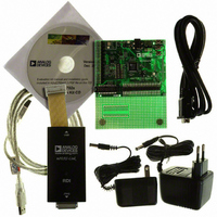
KIT DEV ADUC7026/7027 QUICK PLUS
Manufacturer
Analog Devices Inc
Series
QuickStart™ PLUS Kitr
Type
MCUr
Specifications of EVAL-ADUC7026QSPZ
Contents
Evaluation Board, Power Supply, Cable, Software, Emulator and Documentation
Silicon Manufacturer
Analog Devices
Core Architecture
ARM
Core Sub-architecture
ARM7TDMI
Silicon Core Number
ADuC7026
Rohs Compliant
Yes
Lead Free Status / RoHS Status
Lead free / RoHS Compliant
For Use With/related Products
ADuC7026
Lead Free Status / Rohs Status
Compliant
Available stocks
Company
Part Number
Manufacturer
Quantity
Price
Company:

Part Number:
EVAL-ADUC7026QSPZ
Manufacturer:
Analog Devices Inc
Quantity:
135


Timer0 (RTOS Timer)
Timer0 is a general-purpose, 16-bit timer (count-down) with a
programmable prescaler (see Figure 64). The prescaler source is
the core clock frequency (HCLK) and can be scaled by factors
of 1, 16, or 256.
Timer0 can be used to start ADC conversions as shown in the
block diagram in Figure 64.
Timer0’s interface consists of four MMRs: T0LD, T0VAL,
T0CON, and T0CLRI.
T0LD Register
Name
T0LD
T0LD is a 16-bit load register.
T0VAL Register
Name
T0VAL
T0VAL is a 16-bit read-only register representing the current
state of the counter.
T0CON Register
Name
T0CON
T0CON is the configuration MMR described in Table 75.
Table 75. T0CON MMR Bit Descriptions
Bit
31:8
7
6
5:4
3:2
1:0
HCLK
Value
00
01
10
11
PRESCALER
/1, 16 OR 256
Address
0xFFFF0300
Address
0xFFFF0304
Address
0xFFFF0308
Figure 64. Timer0 Block Diagram
Description
Reserved.
Timer0 Enable Bit. Set by user to enable Timer0.
Cleared by user to disable Timer0 by default.
Timer0 Mode. Set by user to operate in
periodic mode. Cleared by user to operate
in free-running mode. Default mode.
Reserved.
Prescale.
Core Clock/1. Default value.
Core Clock/16.
Core Clock/256.
Undefined. Equivalent to 00.
Reserved.
COUNTER
TIMER0
VALUE
16-BIT
16-BIT
DOWN
LOAD
Default Value
0x0000
Default Value
0xFFFF
Default Value
0x0000
TIMER0 IRQ
ADC CONVERSION
Access
R/W
Access
R
Access
R/W
Rev. B | Page 77 of 92
T0CLRI Register
Name
T0CLRI
T0CLRI is an 8-bit register. Writing any value to this register
clears the interrupt.
Timer1 (General-Purpose Timer)
Timer1 is a general-purpose, 32-bit timer (count down or count
up) with a programmable prescaler. The source can be the
32 kHz external crystal, the core clock frequency, or an external
GPIO, P1.0 or P0.6 (maximum frequency 44 Mhz). This source
can be scaled by a factor of 1, 16, 256, or 32,768.
The counter can be formatted as a standard 32-bit value or as
hours: minutes: seconds: hundredths.
Timer1 has a capture register (T1CAP) that can be triggered by
a selected IRQ source initial assertion. This feature can be used
to determine the assertion of an event more accurately than the
precision allowed by the RTOS timer when the IRQ is serviced.
Timer1 can be used to start ADC conversions as shown in the
block diagram in Figure 65.
32kHz OSCILLATOR
Timer1’s interface consists of five MMRs: T1LD, T1VAL,
T1CON, T1CLRI, and T1CAP.
T1LD Register
Name
T1LD
T1LD is a 32-bit load register.
T1VAL Register
Name
T1VAL
T1VAL is a 32-bit read-only register that represents the current
state of the counter.
T1CON Register
Name
T1CON
T1CON is the configuration MMR described in Table 76.
ADuC7019/20/21/22/24/25/26/27/28
HCLK
P0.6
P1.0
Address
0xFFFF030C
Address
0xFFFF0320
Address
0xFFFF0324
Address
0xFFFF0328
Figure 65. Timer1 Block Diagram
IRQ[31:0]
PRESCALER
/1, 16, 256
OR 32768
Default Value
0xFF
Default Value
0x00000000
Default Value
0xFFFFFFFF
Default Value
0x0000
COUNTER
UP/DOWN
CAPTURE
32-BIT
32-BIT
LOAD
TIMER1
VALUE
TIMER1 IRQ
ADC CONVERSION
Access
W
Access
R/W
Access
R
Access
R/W
Related parts for EVAL-ADUC7026QSPZ
Image
Part Number
Description
Manufacturer
Datasheet
Request
R

Part Number:
Description:
IC, ADJ LDO REG, 1.5V TO 5V 250mA MSOP-8
Manufacturer:
Vishay
Datasheet:

Part Number:
Description:
IC, ADJ LDO REG, 1.5V TO 5V 0.6A 8-TSSOP
Manufacturer:
Vishay
Datasheet:
Part Number:
Description:
IC, ADJ LDO REG, 1.5V TO 5V 250mA MSOP-8
Manufacturer:
Vishay
Datasheet:

Part Number:
Description:
IC ADJ LDO REG 1.5V TO 5V 150mA 5-SOT-23
Manufacturer:
Vishay
Datasheet:

Part Number:
Description:
BOARD EVAL AS1324-AD
Manufacturer:
austriamicrosystems
Datasheet:
Part Number:
Description:
IC, ADJ LDO REG, 1.5V TO 5V 0.6A 8-TSSOP
Manufacturer:
Vishay
Datasheet:

Part Number:
Description:
IC, ADJ LDO REG, 1.5V TO 5V, 0.3A, MSOP8
Manufacturer:
Vishay
Datasheet:
Part Number:
Description:
IC, ADJ LDO REG, 1.5V TO 5V, 0.3A, MSOP8
Manufacturer:
Vishay
Datasheet:
Part Number:
Description:
IC, ADJ LDO REG 1.215V TO 5V 0.3A MSOP-8
Manufacturer:
Vishay
Datasheet:
Part Number:
Description:
IC, ADJ LDO REG 1.215V TO 5V 0.3A MSOP-8
Manufacturer:
Vishay
Datasheet:

Part Number:
Description:
±1.7g Dual-Axis IMEMS Accelerometer Evaluation Board
Manufacturer:
Analog Devices Inc
Datasheet:

Part Number:
Description:
IC MULTIPLIER ANALOG 8-SOIC T/R
Manufacturer:
Analog Devices Inc
Datasheet:

Part Number:
Description:
IC ANALOG MULTIPLIER 8-DIP
Manufacturer:
Analog Devices Inc
Datasheet:
Part Number:
Description:
IC ANALOG MULTIPLIER 8-SOIC
Manufacturer:
Analog Devices Inc
Datasheet:
Part Number:
Description:
IC ANALOG MULTIPLIER 8-DIP
Manufacturer:
Analog Devices Inc
Datasheet: