DEMO9S12XEP100 Freescale Semiconductor, DEMO9S12XEP100 Datasheet - Page 131
DEMO9S12XEP100
Manufacturer Part Number
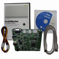
DEMO9S12XEP100
Description
BOARD DEMO FOR MC9S12XEP100
Manufacturer
Freescale Semiconductor
Type
MCUr
Datasheet
1.EVB9S12XEP100.pdf
(1328 pages)
Specifications of DEMO9S12XEP100
Contents
Board, Cables, CD
Processor To Be Evaluated
MC9S12XEP100
Data Bus Width
16 bit
Interface Type
RS-232
Silicon Manufacturer
Freescale
Core Architecture
S12
Core Sub-architecture
S12
Silicon Core Number
MC9S12
Silicon Family Name
S12XE
Rohs Compliant
Yes
For Use With/related Products
MC9S12XEP100
Lead Free Status / RoHS Status
Lead free / RoHS Compliant
Available stocks
Company
Part Number
Manufacturer
Quantity
Price
Company:

Part Number:
DEMO9S12XEP100
Manufacturer:
PANASONIC
Quantity:
46 000
Company:
Part Number:
DEMO9S12XEP100
Manufacturer:
Freescale Semiconductor
Quantity:
135


1. Read: Anytime.
2.3.32
Freescale Semiconductor
Address 0x024B
Write: Anytime.
DDRS
RDRS
Field
Field
Reset
7-0
7-0
W
R
Port S data direction—
This register controls the data direction of pins 7 through 0.This register configures each Port S pin as either input
or output.
If SPI0 is enabled, the SPI0 determines the pin direction. Refer to SPI section for details.
If the associated SCI transmit or receive channel is enabled this register has no effect on the pins. The pin is forced
to be an output if a SCI transmit channel is enabled, it is forced to be an input if the SCI receive channel is enabled.
The data direction bits revert to controlling the I/O direction of a pin when the associated channel is disabled.
1 Associated pin is configured as output.
0 Associated pin is configured as input.
Port S reduced drive—Select reduced drive for outputs
This register configures the drive strength of output pins 7 through 0 as either full or reduced independent of the
function used on the pins. If a pin is used as input this bit has no effect.
1 Reduced drive selected (approx. 1/5 of the full drive strength).
0 Full drive strength enabled.
RDRS7
Port S Reduced Drive Register (RDRS)
0
7
Due to internal synchronization circuits, it can take up to 2 bus clock cycles
until the correct value is read on PTS or PTIS registers, when changing the
DDRS register.
RDRS6
0
6
Figure 2-30. Port S Reduced Drive Register (RDRS)
Table 2-28. DDRS Register Field Descriptions
Table 2-29. RDRS Register Field Descriptions
MC9S12XE-Family Reference Manual , Rev. 1.23
RDRS5
0
5
RDRS4
NOTE
0
4
Description
Description
RDRS3
3
0
Chapter 2 Port Integration Module (S12XEPIMV1)
RDRS2
0
2
Access: User read/write
RDRS1
0
1
RDRS0
0
0
131
(1)
Related parts for DEMO9S12XEP100
Image
Part Number
Description
Manufacturer
Datasheet
Request
R

Part Number:
Description:
Manufacturer:
Freescale Semiconductor, Inc
Datasheet:
Part Number:
Description:
Manufacturer:
Freescale Semiconductor, Inc
Datasheet:
Part Number:
Description:
Manufacturer:
Freescale Semiconductor, Inc
Datasheet:
Part Number:
Description:
Manufacturer:
Freescale Semiconductor, Inc
Datasheet:
Part Number:
Description:
Manufacturer:
Freescale Semiconductor, Inc
Datasheet:
Part Number:
Description:
Manufacturer:
Freescale Semiconductor, Inc
Datasheet:
Part Number:
Description:
Manufacturer:
Freescale Semiconductor, Inc
Datasheet:
Part Number:
Description:
Manufacturer:
Freescale Semiconductor, Inc
Datasheet:
Part Number:
Description:
Manufacturer:
Freescale Semiconductor, Inc
Datasheet:
Part Number:
Description:
Manufacturer:
Freescale Semiconductor, Inc
Datasheet:
Part Number:
Description:
Manufacturer:
Freescale Semiconductor, Inc
Datasheet:
Part Number:
Description:
Manufacturer:
Freescale Semiconductor, Inc
Datasheet:
Part Number:
Description:
Manufacturer:
Freescale Semiconductor, Inc
Datasheet:
Part Number:
Description:
Manufacturer:
Freescale Semiconductor, Inc
Datasheet:
Part Number:
Description:
Manufacturer:
Freescale Semiconductor, Inc
Datasheet: