DEMO9S08DZ60 Freescale Semiconductor, DEMO9S08DZ60 Datasheet - Page 343
DEMO9S08DZ60
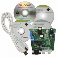
Manufacturer Part Number
DEMO9S08DZ60
Description
BOARD DEMO
Manufacturer
Freescale Semiconductor
Type
MCUr
Datasheets
1.DEMO9S08DZ60.pdf
(416 pages)
2.DEMO9S08DZ60.pdf
(1 pages)
3.DEMO9S08DZ60.pdf
(16 pages)
4.DEMO9S08DZ60.pdf
(2 pages)
5.DEMO9S08DZ60.pdf
(1 pages)
Specifications of DEMO9S08DZ60
Contents
Board, Cable, CD
Processor To Be Evaluated
MC9S08DZ60
Interface Type
RS-232, USB
Silicon Manufacturer
Freescale
Core Architecture
HCS08
Core Sub-architecture
HCS08
Silicon Core Number
MC9S08
Silicon Family Name
S08D
Kit Contents
MC9S08DZ60 Board, Software, Cables, Connectors
Rohs Compliant
Yes
For Use With/related Products
MC9S08DZ60
Lead Free Status / RoHS Status
Lead free / RoHS Compliant


Freescale Semiconductor
3. Read of TPMxCnVH:L registers
4. Write to TPMxCnVH:L registers
— This read coherency mechanism is cleared in TPM v3 in BDM mode if there is a write to
(TPMxCnVH:TPMxCnVL))
— In TPM v3, any read of TPMxCnVH:L registers during BDM mode returns the value of the
— This read coherency mechanism is cleared in TPM v3 in BDM mode if there is a write to
— Input Capture Mode
— Output Compare Mode
— Edge-Aligned PWM
BDM mode returns the latched value of TPMxCNTH:L from the read buffer instead of the
frozen TPM counter value.
TPMxSC, TPMxCNTH or TPMxCNTL. Instead, in these conditions the TPM v2 does not clear
this read coherency mechanism.
TPMxCnVH:L register. In TPM v2, if only one byte of the TPMxCnVH:L registers was read
before the BDM mode became active, then any read of TPMxCnVH:L registers during BDM
mode returns the latched value of TPMxCNTH:L from the read buffer instead of the value in
the TPMxCnVH:L registers.
TPMxCnSC. Instead, in this condition the TPM v2 does not clear this read coherency
mechanism.
In this mode the TPM v3 does not allow the writes to TPMxCnVH:L registers. Instead, the
TPM v2 allows these writes.
In this mode and if (CLKSB:CLKSA not = 0:0), the TPM v3 updates the TPMxCnVH:L
registers with the value of their write buffer at the next change of the TPM counter (end of the
prescaler counting) after the second byte is written. Instead, the TPM v2 always updates these
registers when their second byte is written.
The following procedure can be used in the TPM v3 to verify if the TPMxCnVH:L registers
were updated with the new value that was written to these registers (value in their write buffer).
...
write the new value to TPMxCnVH:L;
read TPMxCnVH and TPMxCnVL registers;
while (the read value of TPMxCnVH:L is different from the new value written to
TPMxCnVH:L)
begin
end
...
In this point, the TPMxCnVH:L registers were updated, so the program can continue and, for
example, write to TPMxC0SC without cancelling the previous write to TPMxCnVH:L
registers.
In this mode and if (CLKSB:CLKSA not = 00), the TPM v3 updates the TPMxCnVH:L
registers with the value of their write buffer after that the both bytes were written and when the
read again TPMxCnVH and TPMxCnVL;
(Section 16.4.2.1, “Input Capture
(Section 16.4.2.3, “Edge-Aligned PWM
(Section 16.4.2.2, “Output Compare
MC9S08DZ60 Series Data Sheet, Rev. 4
(Section 16.3.5, “TPM Channel Value Registers
Mode)
Chapter 16 Timer/PWM Module (S08TPMV3)
Mode)
Mode)
343
Related parts for DEMO9S08DZ60
Image
Part Number
Description
Manufacturer
Datasheet
Request
R

Part Number:
Description:
Manufacturer:
Freescale Semiconductor, Inc
Datasheet:
Part Number:
Description:
Manufacturer:
Freescale Semiconductor, Inc
Datasheet:
Part Number:
Description:
Manufacturer:
Freescale Semiconductor, Inc
Datasheet:
Part Number:
Description:
Manufacturer:
Freescale Semiconductor, Inc
Datasheet:
Part Number:
Description:
Manufacturer:
Freescale Semiconductor, Inc
Datasheet:
Part Number:
Description:
Manufacturer:
Freescale Semiconductor, Inc
Datasheet:
Part Number:
Description:
Manufacturer:
Freescale Semiconductor, Inc
Datasheet:
Part Number:
Description:
Manufacturer:
Freescale Semiconductor, Inc
Datasheet:
Part Number:
Description:
Manufacturer:
Freescale Semiconductor, Inc
Datasheet:
Part Number:
Description:
Manufacturer:
Freescale Semiconductor, Inc
Datasheet:
Part Number:
Description:
Manufacturer:
Freescale Semiconductor, Inc
Datasheet:
Part Number:
Description:
Manufacturer:
Freescale Semiconductor, Inc
Datasheet:
Part Number:
Description:
Manufacturer:
Freescale Semiconductor, Inc
Datasheet:
Part Number:
Description:
Manufacturer:
Freescale Semiconductor, Inc
Datasheet:
Part Number:
Description:
Manufacturer:
Freescale Semiconductor, Inc
Datasheet: