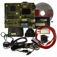
R0K572030S000BE Renesas Electronics America, R0K572030S000BE Datasheet - Page 16

R0K572030S000BE
Manufacturer Part Number
R0K572030S000BE
Description
KIT DEV FOR SH7203
Manufacturer
Renesas Electronics America
Series
Renesas Starter Kits (RSK)r
Type
MCUr
Specifications of R0K572030S000BE
Contents
CPU Board, LCD Module, E10A-Lite Emulator, Cable, QuickStart Guide and CD-ROM
Silicon Manufacturer
Renesas
Kit Contents
Board
Silicon Family Name
SH7203
Silicon Core Number
R5S72030W200FP
Tool / Board Applications
General Purpose MCU, MPU, DSP, DSC
Mcu Supported Families
SH7203
Lead Free Status / RoHS Status
Contains lead / RoHS non-compliant
For Use With/related Products
SH7203
Lead Free Status / Rohs Status
Compliant
SuperH
I
• Compatible with PCI bus operating
• Compatible with 32-bit PCI bus
• Up to four PCI master devices running at
• Arbitration control is available as a PCI
• Can operate as master or target
• When operating as master, PIO and
• Four DMA transfer channels
• Six 32-bit x 16 longword internal FIFO
• SRAM, DRAM, SDRAM, DDR-SDRAM,
• 32-bit or 16-bit memory data bus for data
• Support for big-endian and little-endian
I
• Up to twelve channels
• Choice of 8-bit, 16-bit, 32-bit, 64-bit, or
• Choice of address mode; single or dual;
• Two types of DMAC channel priority
speeds of 33MHz/66MHz
33MHz, or one PCI master device at
66MHz, can be connected
host function
DMA transfer are available
(one for target reading, one for target
writing, and four for DMA transfer)
and MPX can be used as external memory
for PCI bus data transfers
transfers with PCI bus (32-bit bus when
connected to SDRAM or DDR-SDRAM)
local bus (PCI bus operates with little
endian, while internal bus for peripheral
modules operates with big endian)
32-byte transfer data length
choice of bus mode: cycle steal mode or
burst mode
ranking: fixed-priority mode and round-
robin mode
Peripheral Control Interconnect (PCI)
DMA Controller (DMAC)
®
Family of Microcontrollers & Microprocessors
PCI Block Diagram
DMAC: Single and Dual Address Modes
Internal Peripheral
Acknowledge
Bus Request
(Peripheral Bus)
Module Bus
Interrupts
DMAC
DMAC
BSC
BSC
: Data flow
2nd bus cycle: Taking the DAR value as the address, the data stored
in the BSC's data buffer is written to the transfer destination module.
SuperH device
SuperH device
1st bus cycle: Taking the SAR value as the address, data is read
SuperH Device
from the transfer source module and stored temporarily in the
DUAL-ADDRESS MODE: Two-cycle read and write
SINGLE-ADDRESS MODE: Parallel read and write
Data Buffer
Data Buffer
SAR
DA R
SAR
DAR
Module Bus
DMAC
data buffer in the Bus State Controller (BSC).
Peripheral
Interface
Internal
PCIC Module
Interrupt
Control
register
Local
DACK
External
address
bus
Local Bus Clock
(Bf ) Cycle: Bcyc
Local Bus
External
data bus
PCIC Bus Controller
Data Transfer Control
PCI Bus Interface
Register
Register
Register
Local
Local
Local
Transfer Destination
Transfer Destination
Transfer Source
Transfer Source
32B (2 sides) 6
Feedback
Input Clock
from CKIO
Configuration
with DACK
PCI Bus
External
Memory
Memory
Module
Module
External
memory
Module
Module
Register
device
FIFO
PCI
PCI Clock
33/66 MHz
(PCICLK)
14


