MC56F8323EVME Freescale Semiconductor, MC56F8323EVME Datasheet - Page 23
MC56F8323EVME
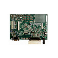
Manufacturer Part Number
MC56F8323EVME
Description
BOARD EVALUATION MC56F8323
Manufacturer
Freescale Semiconductor
Type
DSPr
Specifications of MC56F8323EVME
Contents
Module and Misc Hardware
Processor To Be Evaluated
MC56F8322 and MC56F8323
Data Bus Width
16 bit
Interface Type
RS-232
Silicon Manufacturer
Freescale
Core Architecture
56800/E
Core Sub-architecture
56800/E
Silicon Core Number
MC56F
Silicon Family Name
MC56F83xx
Rohs Compliant
Yes
For Use With/related Products
MC56F8322, MC56F8323
Lead Free Status / RoHS Status
Lead free / RoHS Compliant


Freescale Semiconductor
Preliminary
Signal Name
(prescaler_
(GPIOB4)
(GPIOB3)
(GPIOB2)
HOME0
SCLK0
MOSI0
clock)
(TA3)
Table 2-2 Signal and Package Information for the 64-Pin LQFP
Pin No.
49
25
24
Schmitt
Schmitt
Schmitt
Schmitt
Schmitt
Schmitt
Schmitt
Output
Output
Output
Output
Output
Output
Output
Input/
Input/
Input/
Input/
Input/
Input/
Type
Input
State During
disabled,
pull-up is
output is
In reset,
enabled
enabled
enabled
pull-up
pull-up
Reset
56F8323 Technical Data, Rev. 17
Input,
Input,
Home — Quadrature Decoder 0, HOME input
TA3 — Timer A, Channel 3
Port B GPIO — This GPIO pin can be individually programmed as
an input or output pin.
Clock Output - can be used to monitor the internal prescaler_clock
signal (see
In the 56F8323, the default state after reset is HOME0.
In the 56F8123, the default state is not one of the functions offered
and must be reconfigured.
SPI 0 Serial Clock — In the master mode, this pin serves as an
output, clocking slaved listeners. In slave mode, this pin serves as
the data clock input. A Schmitt trigger input is used for noise
immunity.
Port B GPIO — This GPIO pin can be individually programmed as
an input or output pin.
After reset, the default state is SCLK0.
SPI 0 Master Out/Slave In — This serial data pin is an output from a
master device and an input to a slave device. The master device
places data on the MOSI line a half-cycle before the clock edge the
slave device uses to latch the data.
Port B GPIO — This GPIO pin can be individually programmed as
an input or output pin.
After reset, the default state is MOSI0.
Part 6.5.7
CLKO Select Register, SIM_CLKOSR).
Signal Description
Signal Pins
23
Related parts for MC56F8323EVME
Image
Part Number
Description
Manufacturer
Datasheet
Request
R

Part Number:
Description:
Manufacturer:
Freescale Semiconductor, Inc
Datasheet:
Part Number:
Description:
Manufacturer:
Freescale Semiconductor, Inc
Datasheet:
Part Number:
Description:
Manufacturer:
Freescale Semiconductor, Inc
Datasheet:
Part Number:
Description:
Manufacturer:
Freescale Semiconductor, Inc
Datasheet:
Part Number:
Description:
Manufacturer:
Freescale Semiconductor, Inc
Datasheet:
Part Number:
Description:
Manufacturer:
Freescale Semiconductor, Inc
Datasheet:
Part Number:
Description:
Manufacturer:
Freescale Semiconductor, Inc
Datasheet:
Part Number:
Description:
Manufacturer:
Freescale Semiconductor, Inc
Datasheet:
Part Number:
Description:
Manufacturer:
Freescale Semiconductor, Inc
Datasheet:
Part Number:
Description:
Manufacturer:
Freescale Semiconductor, Inc
Datasheet:
Part Number:
Description:
Manufacturer:
Freescale Semiconductor, Inc
Datasheet:
Part Number:
Description:
Manufacturer:
Freescale Semiconductor, Inc
Datasheet:
Part Number:
Description:
Manufacturer:
Freescale Semiconductor, Inc
Datasheet:
Part Number:
Description:
Manufacturer:
Freescale Semiconductor, Inc
Datasheet:
Part Number:
Description:
Manufacturer:
Freescale Semiconductor, Inc
Datasheet: