MC56F8323EVME Freescale Semiconductor, MC56F8323EVME Datasheet - Page 6
MC56F8323EVME
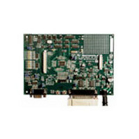
Manufacturer Part Number
MC56F8323EVME
Description
BOARD EVALUATION MC56F8323
Manufacturer
Freescale Semiconductor
Type
DSPr
Specifications of MC56F8323EVME
Contents
Module and Misc Hardware
Processor To Be Evaluated
MC56F8322 and MC56F8323
Data Bus Width
16 bit
Interface Type
RS-232
Silicon Manufacturer
Freescale
Core Architecture
56800/E
Core Sub-architecture
56800/E
Silicon Core Number
MC56F
Silicon Family Name
MC56F83xx
Rohs Compliant
Yes
For Use With/related Products
MC56F8322, MC56F8323
Lead Free Status / RoHS Status
Lead free / RoHS Compliant


Part 1: Overview . . . . . . . . . . . . . . . . . . . . . . . 7
Part 2: Signal/Connection Descriptions . . 16
Part 3: On-Chip Clock Synthesis (OCCS) . . 30
Part 4: Memory Map. . . . . . . . . . . . . . . . . . . 33
Part 5: Interrupt Controller (ITCN) . . . . . . . . 57
Part 6: System Integration Module (SIM) . . 83
Part 7: Security Features . . . . . . . . . . . . . . 99
6
1.1. 56F8323/56F8123 Features . . . . . . . . . . . . . 7
1.2. Device Description . . . . . . . . . . . . . . . . . . . . 9
1.3. Award-Winning Development Environment 10
1.4. Architecture Block Diagram . . . . . . . . . . . . 11
1.5. Product Documentation . . . . . . . . . . . . . . . 15
1.6. Data Sheet Conventions . . . . . . . . . . . . . . . 15
2.1. Introduction . . . . . . . . . . . . . . . . . . . . . . . . . 16
2.2. Signal Pins . . . . . . . . . . . . . . . . . . . . . . . . . 19
3.1. Introduction . . . . . . . . . . . . . . . . . . . . . . . . . 30
3.2. External Clock Operation . . . . . . . . . . . . . . 30
3.3. Use of On-Chip Relaxation Oscillator . . . . . 31
3.4. Internal Clock Operation . . . . . . . . . . . . . . . 32
3.5. Registers . . . . . . . . . . . . . . . . . . . . . . . . . . . 33
4.1. Introduction . . . . . . . . . . . . . . . . . . . . . . . . . 33
4.2. Program Map. . . . . . . . . . . . . . . . . . . . . . . . 33
4.3. Interrupt Vector Table . . . . . . . . . . . . . . . . . 34
4.4. Data Map . . . . . . . . . . . . . . . . . . . . . . . . . . . 37
4.5. Flash Memory Map . . . . . . . . . . . . . . . . . . . 37
4.6. EOnCE Memory Map . . . . . . . . . . . . . . . . . 39
4.7. Peripheral Memory Mapped Registers . . . . 40
4.8. Factory Programmed Memory. . . . . . . . . . . 56
5.1. Introduction . . . . . . . . . . . . . . . . . . . . . . . . . 57
5.2. Features . . . . . . . . . . . . . . . . . . . . . . . . . . . 57
5.3. Functional Description . . . . . . . . . . . . . . . . 57
5.4. Block Diagram . . . . . . . . . . . . . . . . . . . . . . . 59
5.5. Operating Modes . . . . . . . . . . . . . . . . . . . . . 59
5.6. Register Descriptions . . . . . . . . . . . . . . . . . 60
5.7. Resets . . . . . . . . . . . . . . . . . . . . . . . . . . . . 82
6.1. Introduction . . . . . . . . . . . . . . . . . . . . . . . . . 83
6.2. Features . . . . . . . . . . . . . . . . . . . . . . . . . . . 83
6.3. Operating Modes . . . . . . . . . . . . . . . . . . . . 84
6.4. Operating Mode Register . . . . . . . . . . . . . . 84
6.5. Register Descriptions . . . . . . . . . . . . . . . . . 85
6.6. Clock Generation Overview. . . . . . . . . . . . . 97
6.7. Power-Down Modes . . . . . . . . . . . . . . . . . . 97
6.8. Stop and Wait Mode Disable Function . . . . 98
6.9. Resets . . . . . . . . . . . . . . . . . . . . . . . . . . . . . 98
7.1. Operation with Security Enabled . . . . . . . . 99
7.2. Flash Access Blocking Mechanisms . . . . . . 99
56F8323 Technical Data, Rev. 17
Table of Contents
Part 8: General Purpose Input/Output
Part 9: Joint Test Action Group (JTAG) . . 104
Part 10: Specifications. . . . . . . . . . . . . . . . 105
Part 11: Packaging 131
Part 12: Design Considerations . . . . . . . . 136
Part 13: Ordering Information . . . . . . . . . . 139
8.1. Introduction . . . . . . . . . . . . . . . . . . . . . . . . 102
8.2. Configuration. . . . . . . . . . . . . . . . . . . . . . . 102
8.3. Memory Maps . . . . . . . . . . . . . . . . . . . . . . 104
9.1. JTAG Information . . . . . . . . . . . . . . . . . . . 104
10.1. General Characteristics . . . . . . . . . . . . . . 105
10.2. DC Electrical Characteristics. . . . . . . . . . 109
10.3. AC Electrical Characteristics . . . . . . . . . . 113
10.4. Flash Memory Characteristics. . . . . . . . . 114
10.5. External Clock Operation Timing . . . . . . 114
10.6. Phase Locked Loop Timing . . . . . . . . . . . 115
10.7. Crystal Oscillator Parameters . . . . . . . . . 115
10.8. Reset, Stop, Wait, Mode Select, and
10.9. Serial Peripheral Interface (SPI) Timing . . 119
10.10. Quad Timer Timing . . . . . . . . . . . . . . . . 122
10.11. Quadrature Decoder Timing . . . . . . . . . . 122
10.12. Serial Communication Interface
10.13. Controller Area Network (CAN) Timing . 124
10.14. JTAG Timing . . . . . . . . . . . . . . . . . . . . . 124
10.15. Analog-to-Digital Converter
10.16. Equivalent Circuit for ADC Inputs . . . . . 129
10.17. Power Consumption . . . . . . . . . . . . . . . . 129
11.1. 56F8323 Package and Pin-Out
11.2. 56F8123 Package and Pin-Out
12.1. Thermal Design Considerations . . . . . . . 136
12.2. Electrical Design Considerations . . . . . . . 137
12.3. Power Distribution and I/O Ring
(GPIO) . . . . . . . . . . . . . . . . . . . . . . 102
Interrupt Timing . . . . . . . . . . . . . 117
(SCI) Timing . . . . . . . . . . . . . . . . 123
(ADC) Parameters . . . . . . . . . . . 126
Information . . . . . . . . . . . . . . . . . . 131
Information . . . . . . . . . . . . . . . . . 133
Implementation . . . . . . . . . . . . . . 138
Freescale Semiconductor
Preliminary
Related parts for MC56F8323EVME
Image
Part Number
Description
Manufacturer
Datasheet
Request
R

Part Number:
Description:
Manufacturer:
Freescale Semiconductor, Inc
Datasheet:
Part Number:
Description:
Manufacturer:
Freescale Semiconductor, Inc
Datasheet:
Part Number:
Description:
Manufacturer:
Freescale Semiconductor, Inc
Datasheet:
Part Number:
Description:
Manufacturer:
Freescale Semiconductor, Inc
Datasheet:
Part Number:
Description:
Manufacturer:
Freescale Semiconductor, Inc
Datasheet:
Part Number:
Description:
Manufacturer:
Freescale Semiconductor, Inc
Datasheet:
Part Number:
Description:
Manufacturer:
Freescale Semiconductor, Inc
Datasheet:
Part Number:
Description:
Manufacturer:
Freescale Semiconductor, Inc
Datasheet:
Part Number:
Description:
Manufacturer:
Freescale Semiconductor, Inc
Datasheet:
Part Number:
Description:
Manufacturer:
Freescale Semiconductor, Inc
Datasheet:
Part Number:
Description:
Manufacturer:
Freescale Semiconductor, Inc
Datasheet:
Part Number:
Description:
Manufacturer:
Freescale Semiconductor, Inc
Datasheet:
Part Number:
Description:
Manufacturer:
Freescale Semiconductor, Inc
Datasheet:
Part Number:
Description:
Manufacturer:
Freescale Semiconductor, Inc
Datasheet:
Part Number:
Description:
Manufacturer:
Freescale Semiconductor, Inc
Datasheet: