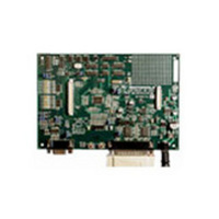
MC56F8323EVME Freescale Semiconductor, MC56F8323EVME Datasheet - Page 95

MC56F8323EVME
Manufacturer Part Number
MC56F8323EVME
Description
BOARD EVALUATION MC56F8323
Manufacturer
Freescale Semiconductor
Type
DSPr
Specifications of MC56F8323EVME
Contents
Module and Misc Hardware
Processor To Be Evaluated
MC56F8322 and MC56F8323
Data Bus Width
16 bit
Interface Type
RS-232
Silicon Manufacturer
Freescale
Core Architecture
56800/E
Core Sub-architecture
56800/E
Silicon Core Number
MC56F
Silicon Family Name
MC56F83xx
Rohs Compliant
Yes
For Use With/related Products
MC56F8322, MC56F8323
Lead Free Status / RoHS Status
Lead free / RoHS Compliant
- Current page: 95 of 140
- Download datasheet (742Kb)
6.5.9.11
Each bit controls clocks to the indicated peripheral.
6.5.9.12
Each bit controls clocks to the indicated peripheral.
6.5.9.13
Each bit controls clocks to the indicated peripheral.
6.5.9.14
This bit field is reserved or not implemented. It is read as 1 and cannot be modified by writing.
6.5.9.15
Each bit controls clocks to the indicated peripheral.
6.5.10
The I/O Short Address Location registers are used to specify the memory referenced via the I/O short
address mode. The I/O short address mode allows the instruction to specify the lower six bits of address;
the upper address bits are not directly controllable. This register set allows limited control of the full
address, as shown in
Note:
Freescale Semiconductor
Preliminary
•
•
•
•
•
•
•
•
1 = Clocks are enabled
0 = The clock is not provided to the peripheral (the peripheral is disabled)
1 = Clocks are enabled
0 = The clock is not provided to the peripheral (the peripheral is disabled)
1 = Clocks are enabled
0 = The clock is not provided to the peripheral (the peripheral is disabled)
1 = Clocks are enabled
0 = The clock is not provided to the peripheral (the peripheral is disabled)
I/O Short Address Location Register (SIM_ISALH and SIM_ISALL)
If this register is set ot something other than the top of memory (EOnCE register space) and the EX bit
in the OMR is set to 1, the JTAG port cannot access the on-chip EOnCE registers, and debug functions
will be affected.
Serial Communications Interface 0 Enable (SCI0)—Bit 4
Serial Peripheral Interface 1 Enable (SPI1)—Bit 3
Serial Peripheral Interface 0 Enable (SPI0)—Bit 2
Reserved—Bit 1
Pulse Width Modulator A Enable (PWMA)—Bit 0
Figure
6-13.
56F8323 Technical Data, Rev. 17
Register Descriptions
95
Related parts for MC56F8323EVME
Image
Part Number
Description
Manufacturer
Datasheet
Request
R
Part Number:
Description:
Manufacturer:
Freescale Semiconductor, Inc
Datasheet:
Part Number:
Description:
Manufacturer:
Freescale Semiconductor, Inc
Datasheet:
Part Number:
Description:
Manufacturer:
Freescale Semiconductor, Inc
Datasheet:
Part Number:
Description:
Manufacturer:
Freescale Semiconductor, Inc
Datasheet:
Part Number:
Description:
Manufacturer:
Freescale Semiconductor, Inc
Datasheet:
Part Number:
Description:
Manufacturer:
Freescale Semiconductor, Inc
Datasheet:
Part Number:
Description:
Manufacturer:
Freescale Semiconductor, Inc
Datasheet:
Part Number:
Description:
Manufacturer:
Freescale Semiconductor, Inc
Datasheet:
Part Number:
Description:
Manufacturer:
Freescale Semiconductor, Inc
Datasheet:
Part Number:
Description:
Manufacturer:
Freescale Semiconductor, Inc
Datasheet:
Part Number:
Description:
Manufacturer:
Freescale Semiconductor, Inc
Datasheet:
Part Number:
Description:
Manufacturer:
Freescale Semiconductor, Inc
Datasheet:
Part Number:
Description:
Manufacturer:
Freescale Semiconductor, Inc
Datasheet:
Part Number:
Description:
Manufacturer:
Freescale Semiconductor, Inc
Datasheet:
Part Number:
Description:
Manufacturer:
Freescale Semiconductor, Inc
Datasheet:


