MCIMX31LITEKITC Freescale Semiconductor, MCIMX31LITEKITC Datasheet - Page 119
MCIMX31LITEKITC
Manufacturer Part Number
MCIMX31LITEKITC
Description
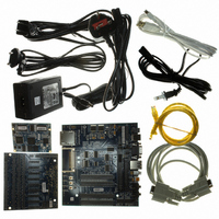
BOARD DEV FOR I.MX31
Manufacturer
Freescale Semiconductor
Type
MCUr
Datasheet
1.MCIMX31LITEKITC.pdf
(122 pages)
Specifications of MCIMX31LITEKITC
Contents
Module and Misc Hardware
For Use With/related Products
i.MX31
Lead Free Status / RoHS Status
Lead free / RoHS Compliant


6
The locations that provide the differences between silicon Revision 2.0, 1.2, and previous versions are
given in
MCIMX31C/MCIMX31LC are outlined in
Freescale Semiconductor
Ordering Information
Feature Differences
Operating Ranges
Power-up
Sequences
Power-down
Sequences
Device ordering
information
Thermal simulation
values
Core overdrive
operating voltages
Fuse_VDD
Ambient operating
temperature range
Current consumption
values
DPLL maximum
output freq range
Item
Item
Product Differences
Table
72. The differences between the MCIMX31/MCIMX31L and the
Section 1.2, “Ordering Information
Table 1.2.1, "Feature Differences
Between Mask Sets," on page 3
Table 4.1, "Chip-Level Conditions,"
on page 10
Section 4.2.1, “Powering Up
Section 4.2.2, “Powering Down
Table 6, "Thermal Resistance
Data—14 × 14 mm Package," on
page 11
Resistance Data—19 × 19 mm
Table 8, "Operating Ranges," on
page 13
Table 8, "Operating Ranges," on
page 13
Operating Ranges for Silicon
Revision 2.0," on page 14
Table 13, "Current Consumption for
–40×C to 85×C, for Silicon Revision
2.0," on page
"Current Consumption for 0×C to
70×C, for Silicon Revision 2.0," on
page 18
Table 13, "Current Consumption for
–40×C to 85×C, for Silicon Revision
2.0," on page 17
Table 31, "DPLL Specifications," on
page 37
Table 1, "Ordering Information," on
page 3
Package," on page 11
Table 72. Silicon Differentiation by Location within the Data Sheet
and
and
Location
Location
Table 7, "Thermal
Table 9, "Specific
17, and
MCIMX31/MCIMX31L Technical Data, Rev. 4.1
Table 73. Product Differentiation
Table 14,
Table
73.
Table 1
N/A
Table 8, "Operating Ranges," on
page 13
Figure 2, "Power-Up Sequence
for Silicon Revisions 1.2 and
Previous," on page 20
See
See
Capability to operate in overdrive
voltages.
Fusebox read Supply Voltage
1.65 min, 1.95 max.
0°C min, 70°C max
–40°C min, 85°C max
Typical value changes for State
Retention, Doze, and Wait. See
Table.
MPLL and SPLL = 532 MHz
Silicon 1.2 and Previous
Table
Table 6
MCIMX31/MCIMX31L
1.
and
—
Table
7.
Table 1
Table 1.2.1
Table
Operating Ranges for Silicon
Revision 2.0," on page 14
Figure 3, "Option 1 Power-Up
Sequence (Silicon Revision
2.0)," on page 21
See
See
Not capable of overdrive
operating voltages.
In read mode, FUSE_VDD
should be floated.
–40°C min, 85°C max
Typical value changes for State
Retention, Doze, and Wait. See
Table.
MPLL and SPLL = 400 MHz
MCIMX31C/MCIMX31LC
Table
Table
8, and
Silicon 2.0
1.
7.
Product Differences
Table 9, "Specific
—
119
Related parts for MCIMX31LITEKITC
Image
Part Number
Description
Manufacturer
Datasheet
Request
R

Part Number:
Description:
Multimedia Applications Processors
Manufacturer:
FREESCALE [Freescale Semiconductor, Inc]
Datasheet:

Part Number:
Description:
Manufacturer:
Freescale Semiconductor, Inc
Datasheet:
Part Number:
Description:
Manufacturer:
Freescale Semiconductor, Inc
Datasheet:
Part Number:
Description:
Manufacturer:
Freescale Semiconductor, Inc
Datasheet:
Part Number:
Description:
Manufacturer:
Freescale Semiconductor, Inc
Datasheet:
Part Number:
Description:
Manufacturer:
Freescale Semiconductor, Inc
Datasheet:
Part Number:
Description:
Manufacturer:
Freescale Semiconductor, Inc
Datasheet:
Part Number:
Description:
Manufacturer:
Freescale Semiconductor, Inc
Datasheet:
Part Number:
Description:
Manufacturer:
Freescale Semiconductor, Inc
Datasheet:
Part Number:
Description:
Manufacturer:
Freescale Semiconductor, Inc
Datasheet:
Part Number:
Description:
Manufacturer:
Freescale Semiconductor, Inc
Datasheet:
Part Number:
Description:
Manufacturer:
Freescale Semiconductor, Inc
Datasheet:
Part Number:
Description:
Manufacturer:
Freescale Semiconductor, Inc
Datasheet:
Part Number:
Description:
Manufacturer:
Freescale Semiconductor, Inc
Datasheet:
Part Number:
Description:
Manufacturer:
Freescale Semiconductor, Inc
Datasheet: