MCIMX31LITEKITC Freescale Semiconductor, MCIMX31LITEKITC Datasheet - Page 43
MCIMX31LITEKITC
Manufacturer Part Number
MCIMX31LITEKITC
Description
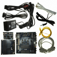
BOARD DEV FOR I.MX31
Manufacturer
Freescale Semiconductor
Type
MCUr
Datasheet
1.MCIMX31LITEKITC.pdf
(122 pages)
Specifications of MCIMX31LITEKITC
Contents
Module and Misc Hardware
For Use With/related Products
i.MX31
Lead Free Status / RoHS Status
Lead free / RoHS Compliant


Figure
basic WEIM accesses to external memory devices with the timing parameters mentioned in
Table 33
Freescale Semiconductor
28,
1
2
3
WE10
WE11
WE18
WE19
WE20
WE22
WE23
WE12
WE13
WE14
WE15
WE16
WE17
WE21
for specific control parameter settings.
WE8
WE9
Applies to rising edge timing
BCLK parameters are being measured from the 50% VDD.
The actual cycle time is derived from the AHB bus clock frequency.
ID
Figure
High is defined as 80% of signal value and low is defined as 20% of signal
value.
Test conditions: load capacitance, 25 pF. Recommended drive strength for all
controls, address, and BCLK is Max drive.
Clock rise to Output Data Invalid
Clock rise to Input Data Invalid, FCE=0
Clock rise/fall to OE Invalid
Clock rise/fall to EB[x] Valid
Clock rise/fall to EB[x] Invalid
Clock rise/fall to LBA Valid
Clock rise/fall to LBA Invalid
Clock rise/fall to Output Data Valid
Input Data Valid to Clock rise, FCE=0
ECB setup time, FCE=0
ECB hold time, FCE=0
DTACK setup time
DTACK hold time
BCLK High Level Width
BCLK Low Level Width
BCLK Cycle time
29,
Figure
Table 33. WEIM Bus Timing Parameters (continued)
30,
FCE=1
FCE=1
1
2
1
Figure
MCIMX31/MCIMX31L Technical Data, Rev. 4.1
2, 3
2, 3
Parameter
31,
FCE=1
FCE=1
Figure
NOTE
32, and
Figure 33
depict some examples of
–2.5
–2.5
Min
2.5
6.5
3.5
4.5
–3
–3
–3
–3
–3
–2
–2
–2
—
—
15
8
2
0
T/2 – 3
T/2 – 3
Electrical Characteristics
Max
—
—
—
—
—
—
—
3
3
3
3
3
4
4
Unit
ns
ns
ns
ns
ns
ns
ns
ns
ns
ns
ns
ns
ns
ns
ns
ns
43
Related parts for MCIMX31LITEKITC
Image
Part Number
Description
Manufacturer
Datasheet
Request
R

Part Number:
Description:
Multimedia Applications Processors
Manufacturer:
FREESCALE [Freescale Semiconductor, Inc]
Datasheet:

Part Number:
Description:
Manufacturer:
Freescale Semiconductor, Inc
Datasheet:
Part Number:
Description:
Manufacturer:
Freescale Semiconductor, Inc
Datasheet:
Part Number:
Description:
Manufacturer:
Freescale Semiconductor, Inc
Datasheet:
Part Number:
Description:
Manufacturer:
Freescale Semiconductor, Inc
Datasheet:
Part Number:
Description:
Manufacturer:
Freescale Semiconductor, Inc
Datasheet:
Part Number:
Description:
Manufacturer:
Freescale Semiconductor, Inc
Datasheet:
Part Number:
Description:
Manufacturer:
Freescale Semiconductor, Inc
Datasheet:
Part Number:
Description:
Manufacturer:
Freescale Semiconductor, Inc
Datasheet:
Part Number:
Description:
Manufacturer:
Freescale Semiconductor, Inc
Datasheet:
Part Number:
Description:
Manufacturer:
Freescale Semiconductor, Inc
Datasheet:
Part Number:
Description:
Manufacturer:
Freescale Semiconductor, Inc
Datasheet:
Part Number:
Description:
Manufacturer:
Freescale Semiconductor, Inc
Datasheet:
Part Number:
Description:
Manufacturer:
Freescale Semiconductor, Inc
Datasheet:
Part Number:
Description:
Manufacturer:
Freescale Semiconductor, Inc
Datasheet: