MCIMX31LITEKITC Freescale Semiconductor, MCIMX31LITEKITC Datasheet - Page 78
MCIMX31LITEKITC
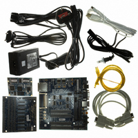
Manufacturer Part Number
MCIMX31LITEKITC
Description
BOARD DEV FOR I.MX31
Manufacturer
Freescale Semiconductor
Type
MCUr
Datasheet
1.MCIMX31LITEKITC.pdf
(122 pages)
Specifications of MCIMX31LITEKITC
Contents
Module and Misc Hardware
For Use With/related Products
i.MX31
Lead Free Status / RoHS Status
Lead free / RoHS Compliant


Electrical Characteristics
The DISP#_IF_CLK_PER_WR, DISP#_IF_CLK_PER_RD, HSP_CLK_PERIOD,
DISP#_IF_CLK_DOWN_WR, DISP#_IF_CLK_UP_WR, DISP#_IF_CLK_DOWN_RD,
DISP#_IF_CLK_UP_RD and DISP#_READ_EN parameters are programmed via the
DI_DISP#_TIME_CONF_1, DI_DISP#_TIME_CONF_2 and DI_HSP_CLK_PER Registers.
4.3.15.5.3
The IPU supports the following types of asynchronous serial interfaces:
Figure 61
DISPB_D#_CS signal and the straight polarity of the DISPB_SD_D_CLK signal.
For this interface, a bidirectional data line is used outside the device. The IPU still uses separate input and
output data lines (IPP_IND_DISPB_SD_D and IPP_DO_DISPB_SD_D). The I/O mux should provide
joining the internal data lines to the bidirectional external line according to the IPP_OBE_DISPB_SD_D
signal provided by the IPU.
Each data transfer can be preceded by an optional preamble with programmable length and contents. The
preamble is followed by read/write (RW) and address (RS) bits. The order of the these bits is
programmable. The RW bit can be disabled. The following data can consist of one word or of a whole
burst. The interface parameters are controlled by the DI_SER_DISP1_CONF and DI_SER_DISP2_CONF
Registers.
Figure 62
data lines both inside and outside the device.
78
DISPB_SD_D_CLK
DISPB_D#_CS
DISPB_SD_D
•
•
•
•
3-wire (with bidirectional data line)
4-wire (with separate data input and output lines)
5-wire type 1 (with sampling RS by the serial clock)
5-wire type 2 (with sampling RS by the chip select signal)
depicts timing of the 4-wire serial interface. For this interface, there are separate input and output
depicts timing of the 3-wire serial interface. The timing images correspond to active-low
Serial Interfaces
1 display IF
clock cycle
Figure 61. 3-Wire Serial Interface Timing Diagram
Preamble
MCIMX31/MCIMX31L Technical Data, Rev. 4.1
, Functional Description
RW
RS
D7
D6
D5
Input or output data
D4
D3
Freescale Semiconductor
D2
1 display IF
clock cycle
D1
D0
Related parts for MCIMX31LITEKITC
Image
Part Number
Description
Manufacturer
Datasheet
Request
R

Part Number:
Description:
Multimedia Applications Processors
Manufacturer:
FREESCALE [Freescale Semiconductor, Inc]
Datasheet:

Part Number:
Description:
Manufacturer:
Freescale Semiconductor, Inc
Datasheet:
Part Number:
Description:
Manufacturer:
Freescale Semiconductor, Inc
Datasheet:
Part Number:
Description:
Manufacturer:
Freescale Semiconductor, Inc
Datasheet:
Part Number:
Description:
Manufacturer:
Freescale Semiconductor, Inc
Datasheet:
Part Number:
Description:
Manufacturer:
Freescale Semiconductor, Inc
Datasheet:
Part Number:
Description:
Manufacturer:
Freescale Semiconductor, Inc
Datasheet:
Part Number:
Description:
Manufacturer:
Freescale Semiconductor, Inc
Datasheet:
Part Number:
Description:
Manufacturer:
Freescale Semiconductor, Inc
Datasheet:
Part Number:
Description:
Manufacturer:
Freescale Semiconductor, Inc
Datasheet:
Part Number:
Description:
Manufacturer:
Freescale Semiconductor, Inc
Datasheet:
Part Number:
Description:
Manufacturer:
Freescale Semiconductor, Inc
Datasheet:
Part Number:
Description:
Manufacturer:
Freescale Semiconductor, Inc
Datasheet:
Part Number:
Description:
Manufacturer:
Freescale Semiconductor, Inc
Datasheet:
Part Number:
Description:
Manufacturer:
Freescale Semiconductor, Inc
Datasheet: