MCIMX31LITEKITC Freescale Semiconductor, MCIMX31LITEKITC Datasheet - Page 58
MCIMX31LITEKITC
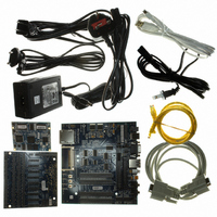
Manufacturer Part Number
MCIMX31LITEKITC
Description
BOARD DEV FOR I.MX31
Manufacturer
Freescale Semiconductor
Type
MCUr
Datasheet
1.MCIMX31LITEKITC.pdf
(122 pages)
Specifications of MCIMX31LITEKITC
Contents
Module and Misc Hardware
For Use With/related Products
i.MX31
Lead Free Status / RoHS Status
Lead free / RoHS Compliant


Electrical Characteristics
4.3.14.2.2
The SENSB_VSYNC, SENSB_HSYNC, and SENSB_PIX_CLK signals are used in this mode. See
Figure
A frame starts with a rising edge on SENSB_VSYNC (all the timings correspond to straight polarity of the
corresponding signals). Then SENSB_HSYNC goes to high and hold for the entire line. Pixel clock is valid
as long as SENSB_HSYNC is high. Data is latched at the rising edge of the valid pixel clocks.
SENSB_HSYNC goes to low at the end of line. Pixel clocks then become invalid and the CSI stops
receiving data from the stream. For next line the SENSB_HSYNC timing repeats. For next frame the
SENSB_VSYNC timing repeats.
4.3.14.2.3
The timing is the same as the gated-clock mode (described in
except for the SENSB_HSYNC signal, which is not used. See
valid and will cause data to be latched into the input FIFO. The SENSB_PIX_CLK signal is inactive (states
low) until valid data is going to be transmitted over the bus.
58
43.
SENSB_DATA[9:0]
SENSB_PIX_CLK
SENSB_DATA[7:0]
SENSB_HSYNC
SENSB_VSYNC
SENSB_PIX_CLK
SENSB_VSYNC
Gated Clock Mode
Non-Gated Clock Mode
Start of Frame
Start of Frame
invalid
invalid
Figure 44. Non-Gated Clock Mode Timing Diagram
nth frame
nth frame
Figure 43. Gated Clock Mode Timing Diagram
MCIMX31/MCIMX31L Technical Data, Rev. 4.1
1st byte
1st byte
Active Line
n+1th frame
invalid
n+1th frame
Section 4.3.14.2.2, “Gated Clock
invalid
Figure
44. All incoming pixel clocks are
1st byte
1st byte
Freescale Semiconductor
Mode”),
Related parts for MCIMX31LITEKITC
Image
Part Number
Description
Manufacturer
Datasheet
Request
R

Part Number:
Description:
Multimedia Applications Processors
Manufacturer:
FREESCALE [Freescale Semiconductor, Inc]
Datasheet:

Part Number:
Description:
Manufacturer:
Freescale Semiconductor, Inc
Datasheet:
Part Number:
Description:
Manufacturer:
Freescale Semiconductor, Inc
Datasheet:
Part Number:
Description:
Manufacturer:
Freescale Semiconductor, Inc
Datasheet:
Part Number:
Description:
Manufacturer:
Freescale Semiconductor, Inc
Datasheet:
Part Number:
Description:
Manufacturer:
Freescale Semiconductor, Inc
Datasheet:
Part Number:
Description:
Manufacturer:
Freescale Semiconductor, Inc
Datasheet:
Part Number:
Description:
Manufacturer:
Freescale Semiconductor, Inc
Datasheet:
Part Number:
Description:
Manufacturer:
Freescale Semiconductor, Inc
Datasheet:
Part Number:
Description:
Manufacturer:
Freescale Semiconductor, Inc
Datasheet:
Part Number:
Description:
Manufacturer:
Freescale Semiconductor, Inc
Datasheet:
Part Number:
Description:
Manufacturer:
Freescale Semiconductor, Inc
Datasheet:
Part Number:
Description:
Manufacturer:
Freescale Semiconductor, Inc
Datasheet:
Part Number:
Description:
Manufacturer:
Freescale Semiconductor, Inc
Datasheet:
Part Number:
Description:
Manufacturer:
Freescale Semiconductor, Inc
Datasheet: