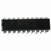
MC68HC908JB8JPE Freescale Semiconductor, MC68HC908JB8JPE Datasheet - Page 166

MC68HC908JB8JPE
Manufacturer Part Number
MC68HC908JB8JPE
Description
IC MCU FLASH 8BIT 8K 20-DIP
Manufacturer
Freescale Semiconductor
Series
HC08r
Datasheet
1.MC908JB8JDWE.pdf
(286 pages)
Specifications of MC68HC908JB8JPE
Core Processor
HC08
Core Size
8-Bit
Speed
3MHz
Connectivity
USB
Peripherals
LVD, POR, PWM
Number Of I /o
13
Program Memory Size
8KB (8K x 8)
Program Memory Type
FLASH
Ram Size
256 x 8
Voltage - Supply (vcc/vdd)
4 V ~ 5.5 V
Oscillator Type
Internal
Operating Temperature
0°C ~ 70°C
Package / Case
20-DIP (0.300", 7.62mm)
Controller Family/series
HC08
No. Of I/o's
13
Ram Memory Size
256Byte
Cpu Speed
3MHz
No. Of Timers
1
Embedded Interface Type
USB
Rohs Compliant
Yes
Processor Series
HC08JB
Core
HC08
Data Bus Width
8 bit
Data Ram Size
256 B
Interface Type
USB
Maximum Clock Frequency
3 MHz
Number Of Programmable I/os
37
Number Of Timers
2
Operating Supply Voltage
4 V to 5.5 V
Maximum Operating Temperature
+ 70 C
Mounting Style
Through Hole
Development Tools By Supplier
FSICEBASE, DEMO908GZ60E, M68EML08GZE, KITUSBSPIDGLEVME, KITUSBSPIEVME, KIT33810EKEVME
Minimum Operating Temperature
0 C
Lead Free Status / RoHS Status
Lead free / RoHS Compliant
Eeprom Size
-
Data Converters
-
Lead Free Status / Rohs Status
Details
- Current page: 166 of 286
- Download datasheet (2Mb)
Monitor ROM (MON)
10.4.1 Entering Monitor Mode
Technical Data
166
V
V
DD
DD
Notes:
1. PTA3 = 0: Bypasses the divide-by-two prescaler to SIM when using V
2. See
V
V
DD
DD
+ V
+ V
Section 18. Electrical Specifications
HI
HI
(contain
BLANK
BLANK
$FF)
NOT
X
X
Table 10-1. Mode Entry Requirements and Options
X
X
0
1
Table 10-1
specified in the table, monitor mode may be entered after a POR and will
allow communication at 9600 baud provided one of the following sets of
conditions is met:
1. If IRQ = V
2. If IRQ = V
3. If $FFFE & $FFFF is blank (contains $FF):
X
X
0
0
– External clock on OSC1 is 3MHz
– PTA3 = low
– External clock on OSC1 is 6MHz
– PTA3 = high
– External clock on OSC1 is 6MHz
– IRQ = V
X
X
1
1
X
1
1
1
shows the pin conditions for entering monitor mode. As
for V
Monitor ROM (MON)
External Clock,
DD
DD
DD
DD
+ V
+ V
+ V
3MHz
6MHz
6MHz
6MHz
f
MC68HC908JB8•MC68HC08JB8•MC68HC08JT8 — Rev. 2.3
XCLK
HI
voltage level requirements.
HI
HI
:
:
DD
Frequency,
(f
(f
(f
+ V
XCLK
XCLK
XCLK
(f
3MHz
3MHz
3MHz
3MHz
f
Bus
XCLK
BUS
HI
for monitor mode entry.
÷ 2)
÷ 2)
÷ 2)
)
High-voltage entry to
monitor mode.
9600 baud communication
on PTA0. COP disabled.
Low-voltage entry to
monitor mode.
9600 baud communication
on PTA0. COP disabled.
Enters user mode.
If $FFFE and $FFFF is
blank, MCU will encounter
an illegal address reset.
Freescale Semiconductor
Comments
Related parts for MC68HC908JB8JPE
Image
Part Number
Description
Manufacturer
Datasheet
Request
R
Part Number:
Description:
Manufacturer:
Freescale Semiconductor, Inc
Datasheet:
Part Number:
Description:
Manufacturer:
Freescale Semiconductor, Inc
Datasheet:
Part Number:
Description:
Manufacturer:
Freescale Semiconductor, Inc
Datasheet:
Part Number:
Description:
Manufacturer:
Freescale Semiconductor, Inc
Datasheet:
Part Number:
Description:
Manufacturer:
Freescale Semiconductor, Inc
Datasheet:
Part Number:
Description:
Manufacturer:
Freescale Semiconductor, Inc
Datasheet:
Part Number:
Description:
Manufacturer:
Freescale Semiconductor, Inc
Datasheet:
Part Number:
Description:
Manufacturer:
Freescale Semiconductor, Inc
Datasheet:
Part Number:
Description:
Manufacturer:
Freescale Semiconductor, Inc
Datasheet:
Part Number:
Description:
Manufacturer:
Freescale Semiconductor, Inc
Datasheet:
Part Number:
Description:
Manufacturer:
Freescale Semiconductor, Inc
Datasheet:
Part Number:
Description:
Manufacturer:
Freescale Semiconductor, Inc
Datasheet:
Part Number:
Description:
Manufacturer:
Freescale Semiconductor, Inc
Datasheet:
Part Number:
Description:
Manufacturer:
Freescale Semiconductor, Inc
Datasheet:
Part Number:
Description:
Manufacturer:
Freescale Semiconductor, Inc
Datasheet:


