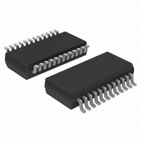
C8051F902-GU Silicon Laboratories Inc, C8051F902-GU Datasheet - Page 36

C8051F902-GU
Manufacturer Part Number
C8051F902-GU
Description
IC MCU 8BIT 8KB FLASH 24QSOP
Manufacturer
Silicon Laboratories Inc
Series
C8051F9xxr
Specifications of C8051F902-GU
Program Memory Type
FLASH
Program Memory Size
8KB (8K x 8)
Package / Case
24-QSOP
Core Processor
8051
Core Size
8-Bit
Speed
25MHz
Connectivity
SMBus (2-Wire/I²C), SPI, UART/USART
Peripherals
Brown-out Detect/Reset, POR, PWM, Temp Sensor, WDT
Number Of I /o
16
Ram Size
768 x 8
Voltage - Supply (vcc/vdd)
0.9 V ~ 3.6 V
Data Converters
A/D 15x10/12b
Oscillator Type
Internal
Operating Temperature
-40°C ~ 85°C
Processor Series
C8051F9x
Core
8051
Data Ram Size
768 B
Interface Type
UART
Maximum Clock Frequency
25 MHz
Number Of Timers
4
Operating Supply Voltage
0.9 V to 3.6 V
Maximum Operating Temperature
+ 85 C
Mounting Style
SMD/SMT
3rd Party Development Tools
PK51, CA51, A51, ULINK2
Development Tools By Supplier
C8051F912DK
Minimum Operating Temperature
- 40 C
On-chip Adc
12 bit
Package
24QSOP
Device Core
8051
Family Name
C8051F90x
Maximum Speed
25 MHz
Data Bus Width
8 Bit
Number Of Programmable I/os
16
Lead Free Status / RoHS Status
Lead free / RoHS Compliant
Eeprom Size
-
Lead Free Status / Rohs Status
Lead free / RoHS Compliant
Other names
336-1849-5
Available stocks
Company
Part Number
Manufacturer
Quantity
Price
Company:
Part Number:
C8051F902-GU
Manufacturer:
SEMIKRON
Quantity:
45
Company:
Part Number:
C8051F902-GU
Manufacturer:
Silicon Laboratories Inc
Quantity:
135
- Current page: 36 of 318
- Download datasheet (3Mb)
C8051F91x-C8051F90x
4.
Throughout the Electrical Characteristics chapter, “VDD” refers to the VDD/DC+ Supply Voltage.
Blue
4.1.
Table 4.1. Absolute Maximum Ratings
36
Ambient temperature under bias
Storage Temperature
Voltage on any Port I/O Pin or
RST with respect to GND
Voltage on VBAT with respect to
GND
Voltage on VDD/DC+ with respect
to GND
Maximum total current through
VBAT, DCEN, VDD/DC+ or GND
Maximum current through RST or
any Port pin
Maximum total current through all
Port pins
DC-DC Converter Output Power
Note: Stresses above those listed under “Absolute Maximum Ratings” may cause permanent damage to the device.
indicates a feature only available on ‘F912 and ‘F902 devices.
Electrical Characteristics
This is a stress rating only and functional operation of the devices at those or any other conditions above those
indicated in the operation listings of this specification is not implied. Exposure to maximum rating conditions for
extended periods may affect device reliability.
Absolute Maximum Specifications
Parameter
VDD > 2.2 V
VDD < 2.2 V
One-Cell Mode (F912/02
One-Cell Mode (F911/01)
Two-Cell Mode
Conditions
Rev. 1.0
–0.3
–0.3
–0.3
–0.3
–0.3
–0.3
Min
–55
–65
—
—
—
—
Typ
—
—
—
—
—
—
—
—
—
—
—
—
VDD + 3.6
Max
125
150
500
100
200
110
4.0
5.8
4.0
2.0
4.0
Units
mW
mA
mA
mA
°C
°C
V
V
V
Related parts for C8051F902-GU
Image
Part Number
Description
Manufacturer
Datasheet
Request
R
Part Number:
Description:
SMD/C°/SINGLE-ENDED OUTPUT SILICON OSCILLATOR
Manufacturer:
Silicon Laboratories Inc
Part Number:
Description:
Manufacturer:
Silicon Laboratories Inc
Datasheet:
Part Number:
Description:
N/A N/A/SI4010 AES KEYFOB DEMO WITH LCD RX
Manufacturer:
Silicon Laboratories Inc
Datasheet:
Part Number:
Description:
N/A N/A/SI4010 SIMPLIFIED KEY FOB DEMO WITH LED RX
Manufacturer:
Silicon Laboratories Inc
Datasheet:
Part Number:
Description:
N/A/-40 TO 85 OC/EZLINK MODULE; F930/4432 HIGH BAND (REV E/B1)
Manufacturer:
Silicon Laboratories Inc
Part Number:
Description:
EZLink Module; F930/4432 Low Band (rev e/B1)
Manufacturer:
Silicon Laboratories Inc
Part Number:
Description:
I°/4460 10 DBM RADIO TEST CARD 434 MHZ
Manufacturer:
Silicon Laboratories Inc
Part Number:
Description:
I°/4461 14 DBM RADIO TEST CARD 868 MHZ
Manufacturer:
Silicon Laboratories Inc
Part Number:
Description:
I°/4463 20 DBM RFSWITCH RADIO TEST CARD 460 MHZ
Manufacturer:
Silicon Laboratories Inc
Part Number:
Description:
I°/4463 20 DBM RADIO TEST CARD 868 MHZ
Manufacturer:
Silicon Laboratories Inc
Part Number:
Description:
I°/4463 27 DBM RADIO TEST CARD 868 MHZ
Manufacturer:
Silicon Laboratories Inc
Part Number:
Description:
I°/4463 SKYWORKS 30 DBM RADIO TEST CARD 915 MHZ
Manufacturer:
Silicon Laboratories Inc
Part Number:
Description:
N/A N/A/-40 TO 85 OC/4463 RFMD 30 DBM RADIO TEST CARD 915 MHZ
Manufacturer:
Silicon Laboratories Inc
Part Number:
Description:
I°/4463 20 DBM RADIO TEST CARD 169 MHZ
Manufacturer:
Silicon Laboratories Inc


