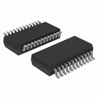
C8051F902-GU Silicon Laboratories Inc, C8051F902-GU Datasheet - Page 78

C8051F902-GU
Manufacturer Part Number
C8051F902-GU
Description
IC MCU 8BIT 8KB FLASH 24QSOP
Manufacturer
Silicon Laboratories Inc
Series
C8051F9xxr
Specifications of C8051F902-GU
Program Memory Type
FLASH
Program Memory Size
8KB (8K x 8)
Package / Case
24-QSOP
Core Processor
8051
Core Size
8-Bit
Speed
25MHz
Connectivity
SMBus (2-Wire/I²C), SPI, UART/USART
Peripherals
Brown-out Detect/Reset, POR, PWM, Temp Sensor, WDT
Number Of I /o
16
Ram Size
768 x 8
Voltage - Supply (vcc/vdd)
0.9 V ~ 3.6 V
Data Converters
A/D 15x10/12b
Oscillator Type
Internal
Operating Temperature
-40°C ~ 85°C
Processor Series
C8051F9x
Core
8051
Data Ram Size
768 B
Interface Type
UART
Maximum Clock Frequency
25 MHz
Number Of Timers
4
Operating Supply Voltage
0.9 V to 3.6 V
Maximum Operating Temperature
+ 85 C
Mounting Style
SMD/SMT
3rd Party Development Tools
PK51, CA51, A51, ULINK2
Development Tools By Supplier
C8051F912DK
Minimum Operating Temperature
- 40 C
On-chip Adc
12 bit
Package
24QSOP
Device Core
8051
Family Name
C8051F90x
Maximum Speed
25 MHz
Data Bus Width
8 Bit
Number Of Programmable I/os
16
Lead Free Status / RoHS Status
Lead free / RoHS Compliant
Eeprom Size
-
Lead Free Status / Rohs Status
Lead free / RoHS Compliant
Other names
336-1849-5
Available stocks
Company
Part Number
Manufacturer
Quantity
Price
Company:
Part Number:
C8051F902-GU
Manufacturer:
SEMIKRON
Quantity:
45
Company:
Part Number:
C8051F902-GU
Manufacturer:
Silicon Laboratories Inc
Quantity:
135
- Current page: 78 of 318
- Download datasheet (3Mb)
C8051F91x-C8051F90x
5.7.
ADC0 on C8051F91x-C8051F90x has an analog multiplexer, referred to as AMUX0.
AMUX0 selects the positive inputs to the single-ended ADC0. Any of the following may be selected as the
positive input: Port I/O pins, the on-chip temperature sensor, the VBAT Power Supply, Regulated Digital
Supply Voltage (Output of VREG0), VDD/DC+ Supply, or the positive input may be connected to GND. The
ADC0 input channels are selected in the ADC0MX register described in SFR Definition 5.12.
Important Note About ADC0 Input Configuration: Port pins selected as ADC0 inputs should be
configured as analog inputs, and should be skipped by the Digital Crossbar. To configure a Port pin for
analog input, set to 0 the corresponding bit in register PnMDIN and disable the digital driver (PnMDOUT =
0 and Port Latch = 1). To force the Crossbar to skip a Port pin, set to 1 the corresponding bit in register
PnSKIP. See Section “21. Port Input/Output” on page 205 for more Port I/O configuration details.
78
ADC0 Analog Multiplexer
Sensor
Sensor
Temp
Temp
Digital Supply
Digital Supply
VDD/DC+
VDD/DC+
P1.6*
P1.6*
P0.0
P0.0
VBAT
VBAT
Figure 5.7. ADC0 Multiplexer Block Diagram
ADC0MX
ADC0MX
AMUX
AMUX
Rev. 1.0
Gain = 0.5 or 1
Gain = 0.5 or 1
Programmable
Programmable
Attenuator
Attenuator
AIN+
AIN+
ADC0
ADC0
Related parts for C8051F902-GU
Image
Part Number
Description
Manufacturer
Datasheet
Request
R
Part Number:
Description:
SMD/C°/SINGLE-ENDED OUTPUT SILICON OSCILLATOR
Manufacturer:
Silicon Laboratories Inc
Part Number:
Description:
Manufacturer:
Silicon Laboratories Inc
Datasheet:
Part Number:
Description:
N/A N/A/SI4010 AES KEYFOB DEMO WITH LCD RX
Manufacturer:
Silicon Laboratories Inc
Datasheet:
Part Number:
Description:
N/A N/A/SI4010 SIMPLIFIED KEY FOB DEMO WITH LED RX
Manufacturer:
Silicon Laboratories Inc
Datasheet:
Part Number:
Description:
N/A/-40 TO 85 OC/EZLINK MODULE; F930/4432 HIGH BAND (REV E/B1)
Manufacturer:
Silicon Laboratories Inc
Part Number:
Description:
EZLink Module; F930/4432 Low Band (rev e/B1)
Manufacturer:
Silicon Laboratories Inc
Part Number:
Description:
I°/4460 10 DBM RADIO TEST CARD 434 MHZ
Manufacturer:
Silicon Laboratories Inc
Part Number:
Description:
I°/4461 14 DBM RADIO TEST CARD 868 MHZ
Manufacturer:
Silicon Laboratories Inc
Part Number:
Description:
I°/4463 20 DBM RFSWITCH RADIO TEST CARD 460 MHZ
Manufacturer:
Silicon Laboratories Inc
Part Number:
Description:
I°/4463 20 DBM RADIO TEST CARD 868 MHZ
Manufacturer:
Silicon Laboratories Inc
Part Number:
Description:
I°/4463 27 DBM RADIO TEST CARD 868 MHZ
Manufacturer:
Silicon Laboratories Inc
Part Number:
Description:
I°/4463 SKYWORKS 30 DBM RADIO TEST CARD 915 MHZ
Manufacturer:
Silicon Laboratories Inc
Part Number:
Description:
N/A N/A/-40 TO 85 OC/4463 RFMD 30 DBM RADIO TEST CARD 915 MHZ
Manufacturer:
Silicon Laboratories Inc
Part Number:
Description:
I°/4463 20 DBM RADIO TEST CARD 169 MHZ
Manufacturer:
Silicon Laboratories Inc


