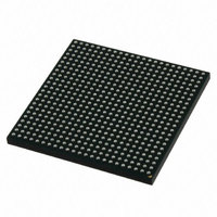
MCIMX512CJM6C Freescale Semiconductor, MCIMX512CJM6C Datasheet - Page 44

MCIMX512CJM6C
Manufacturer Part Number
MCIMX512CJM6C
Description
MULTIMEDIA PROC 529-LFBGA
Manufacturer
Freescale Semiconductor
Series
i.MX51r
Specifications of MCIMX512CJM6C
Core Processor
ARM Cortex-A8
Core Size
32-Bit
Speed
600MHz
Connectivity
1-Wire, EBI/EMI, Ethernet, I²C, IrDA, MMC, SPI, SSI, UART/USART, USB OTG
Peripherals
DMA, I²S, LCD, POR, PWM, WDT
Number Of I /o
128
Program Memory Type
ROMless
Ram Size
128K x 8
Voltage - Supply (vcc/vdd)
0.8 V ~ 1.15 V
Oscillator Type
External
Operating Temperature
-20°C ~ 85°C
Package / Case
529-LFBGA
Operating Temperature (min)
-40C
Operating Temperature Classification
Industrial
Mounting
Surface Mount
Processor Series
i.MX51
Core
ARM Cortex A8
Data Bus Width
32 bit
Program Memory Size
36 KB
Data Ram Size
128 KB
Interface Type
I2C, SPI, SSI, UART, USB
Maximum Clock Frequency
200 MHz
Number Of Timers
5
Operating Supply Voltage
0.8 V to 1.15 V
Maximum Operating Temperature
+ 95 C
Mounting Style
SMD/SMT
3rd Party Development Tools
MDK-ARM, RL-ARM, ULINK2
Development Tools By Supplier
MCIMX51EVKJ
Minimum Operating Temperature
- 40 C
Lead Free Status / RoHS Status
Lead free / RoHS Compliant
Eeprom Size
-
Program Memory Size
-
Data Converters
-
Lead Free Status / Rohs Status
Compliant
- Current page: 44 of 200
- Download datasheet (6Mb)
Electrical Characteristics
AC electrical characteristics in DDR mobile for Fast mode and ovdd=1.65-1.95V, ipp_hve=0 are placed
in
44
1
2
3
Output Pad di/dt
Input Pad Transition Times
Input Pad Propagation Delay (DDR input),
50%-50%
Maximum Input Transition Times
Output Pad Transition Times (High Drive)
Output Pad Transition Times (Medium Drive)
Output Pad Transition Times (Low Drive)
Output Pad Propagation Delay (High Drive)
Output Pad Propagation Delay (Medium Drive)
Output Pad Propagation Delay (Low Drive)
Output Pad Slew Rate (High Drive)
Output Pad Slew Rate (Medium Drive)
Output Pad Slew Rate (Low Drive)
Output Pad di/dt (High Drive)
Output Pad di/dt (Medium drive)
Table
Max condition for tpr, tpo, tps and didt: wcs model, 1.1 V, IO 1.65 V, 105 °C and s0-s5=111111. Typ condition for tpr, tpo,
tps and didt: typ model, 1.2 V, IO 1.8 V, 25 °C and s0-s5=101010. Min condition for tpr, tpo, tps and didt: bcs model, 1.3
V, IO 1.95 V, -40 °C and s0-s5=000000.
Max condition for trfi and tpi: wcs model, 1.1 V, IO 1.65 V and 105 °C. Typ condition for trfi and tpi: typ model, 1.2 V, IO 1.8
V and 25 °C. Min condition for trfi and tpi: bcs model, 1.3 V, IO 1.95 V and -40 °C.
Hysteresis mode is recommended for input with transition time greater than 25 ns.
43.
2
Table 42. AC Electrical Characteristics of DDR2_clk IO Pads for Slow mode and for
Table 43. AC Electrical Characteristics of DDR_clk mobile IO Pads for Fast mode
1
i.MX51 Applications Processors for Consumer and Industrial Products, Rev. 4
Parameter
Parameter
2
1
1
3
1
ovdd=1.65 – 1.95 V (ipp_hve=0) (continued)
1
1
and ovdd=1.65 – 1.95 V (ipp_hve=0)
1
1
1
1
1
1
Symbol
Symbol
di/dt
di/dt
di/dt
trm
tpo
tpo
tpo
tps
tps
tps
tpr
tpr
tpr
trfi
tpi
Condition
Condition
1.2 pF
1.2 pF
15pF
35pF
15pF
35pF
15pF
35pF
15pF
35pF
15pF
35pF
15pF
35pF
15pF
35pF
15pF
35pF
15pF
35pF
Test
Test
—
—
—
—
0.09/0.09 0.132/0.128 0.212/0.213
1.35/1.32
3.01/2.96
1.98/1.98
4.52/4.38
3.99/3.94
8.93/8.86
1.60/1.58
2.74/2.81
2.07/2.08
3.79/3.92
3.47/3.57
6.94/7.26
0.87/0.89
0.39/0.40
0.59/0.59
0.26/0.27
0.29/0.30
0.13/0.13
0.3/0.36
rise/fall
rise/fall
Min
Min
185
124
82
—
1.03/1.03
2.29/2.30
1.55/1.54
3.46/3.45
3.10/3.04
6.77/6.85
1.85/1.74
2.71/2.67
2.19/2.12
3.46/3.51
3.23/3.25
5.84/6.06
1.05/1.05
0.47/0.47
0.70/0.70
0.31/0.31
0.35/0.36
0.16/0.16
0.5/0.52
Typ
Typ
40
61
—
91
Freescale Semiconductor
0.82/0.94
0.89/0.89
1.84/1.92
1.29/1.30
2.80/2.88
2.50/2.57
5.40/5.68
2.58/2.31
3.26/3.08
2.86/2.62
3.87/3.77
3.69/3.55
5.73/5.87
0.54/0.52
0.77/0.76
0.35/0.34
0.40/0.39
0.18/0.17
1.11/1.11
rise/fall
rise/fall
Max
Max
19
46
31
5
mA/ns
mA/ns
mA/ns
Units
Units
V/ns
V/ns
V/ns
ns
ns
ns
ns
ns
ns
ns
ns
ns
Related parts for MCIMX512CJM6C
Image
Part Number
Description
Manufacturer
Datasheet
Request
R
Part Number:
Description:
MCIMX-LVDS1
Manufacturer:
Freescale Semiconductor
Datasheet:
Part Number:
Description:
Manufacturer:
Freescale Semiconductor, Inc
Datasheet:
Part Number:
Description:
Manufacturer:
Freescale Semiconductor, Inc
Datasheet:
Part Number:
Description:
Manufacturer:
Freescale Semiconductor, Inc
Datasheet:
Part Number:
Description:
Manufacturer:
Freescale Semiconductor, Inc
Datasheet:
Part Number:
Description:
Manufacturer:
Freescale Semiconductor, Inc
Datasheet:
Part Number:
Description:
Manufacturer:
Freescale Semiconductor, Inc
Datasheet:
Part Number:
Description:
Manufacturer:
Freescale Semiconductor, Inc
Datasheet:
Part Number:
Description:
Manufacturer:
Freescale Semiconductor, Inc
Datasheet:
Part Number:
Description:
Manufacturer:
Freescale Semiconductor, Inc
Datasheet:
Part Number:
Description:
Manufacturer:
Freescale Semiconductor, Inc
Datasheet:
Part Number:
Description:
Manufacturer:
Freescale Semiconductor, Inc
Datasheet:
Part Number:
Description:
Manufacturer:
Freescale Semiconductor, Inc
Datasheet:
Part Number:
Description:
Manufacturer:
Freescale Semiconductor, Inc
Datasheet:
Part Number:
Description:
Manufacturer:
Freescale Semiconductor, Inc
Datasheet:


