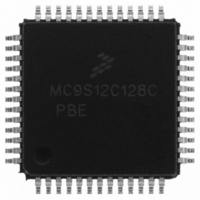
MC9S12C128CPBE Freescale Semiconductor, MC9S12C128CPBE Datasheet - Page 104

MC9S12C128CPBE
Manufacturer Part Number
MC9S12C128CPBE
Description
IC MCU 128K FLASH 25MHZ 52-LQFP
Manufacturer
Freescale Semiconductor
Series
HCS12r
Specifications of MC9S12C128CPBE
Core Processor
HCS12
Core Size
16-Bit
Speed
25MHz
Connectivity
CAN, EBI/EMI, SCI, SPI
Peripherals
POR, PWM, WDT
Number Of I /o
35
Program Memory Size
128KB (128K x 8)
Program Memory Type
FLASH
Ram Size
4K x 8
Voltage - Supply (vcc/vdd)
2.35 V ~ 5.5 V
Data Converters
A/D 8x10b
Oscillator Type
Internal
Operating Temperature
-40°C ~ 85°C
Package / Case
52-LQFP
Lead Free Status / RoHS Status
Lead free / RoHS Compliant
Eeprom Size
-
Available stocks
Company
Part Number
Manufacturer
Quantity
Price
Company:
Part Number:
MC9S12C128CPBE
Manufacturer:
Freescale Semiconductor
Quantity:
10 000
Company:
Part Number:
MC9S12C128CPBER
Manufacturer:
Freescale Semiconductor
Quantity:
10 000
- Current page: 104 of 690
- Download datasheet (4Mb)
Chapter 2 Port Integration Module (PIM9C32) Block Description
2.4
Each pin can act as general purpose I/O. In addition the pin can act as an output from a peripheral module
or an input to a peripheral module.
A set of configuration registers is common to all ports. All registers can be written at any time, however a
specific configuration might not become active.
Example: Selecting a pull-up resistor. This resistor does not become active while the port is used as a push-
pull output.
2.4.1
2.4.1.1
This register holds the value driven out to the pin if the port is used as a general purpose I/O. Writing to
this register has only an effect on the pin if the port is used as general purpose output. When reading this
address, the value of the pins are returned if the data direction register bits are set to 0.
If the data direction register bits are set to 1, the contents of the I/O register is returned. This is independent
of any other configuration
2.4.1.2
This is a read-only register and always returns the value of the pin
2.4.1.3
This register defines whether the pin is used as an input or an output. If a peripheral module controls the
pin the contents of the data direction register is ignored
104
Functional Description
Registers
I/O Register
Input Register
Data Direction Register
(Figure
Figure 2-46. Illustration of I/O Pin Functionality
Module
DDR
PTI
PT
2-46).
MC9S12C-Family / MC9S12GC-Family
Data Out
Output Enable
Module Enable
0
1
Rev 01.24
0
1
0
1
(Figure
2-46).
(Figure
PAD
2-46).
Freescale Semiconductor
Related parts for MC9S12C128CPBE
Image
Part Number
Description
Manufacturer
Datasheet
Request
R
Part Number:
Description:
Manufacturer:
Freescale Semiconductor, Inc
Datasheet:
Part Number:
Description:
Manufacturer:
Freescale Semiconductor, Inc
Datasheet:
Part Number:
Description:
Manufacturer:
Freescale Semiconductor, Inc
Datasheet:
Part Number:
Description:
Manufacturer:
Freescale Semiconductor, Inc
Datasheet:
Part Number:
Description:
Manufacturer:
Freescale Semiconductor, Inc
Datasheet:
Part Number:
Description:
Manufacturer:
Freescale Semiconductor, Inc
Datasheet:
Part Number:
Description:
Manufacturer:
Freescale Semiconductor, Inc
Datasheet:
Part Number:
Description:
Manufacturer:
Freescale Semiconductor, Inc
Datasheet:
Part Number:
Description:
Manufacturer:
Freescale Semiconductor, Inc
Datasheet:
Part Number:
Description:
Manufacturer:
Freescale Semiconductor, Inc
Datasheet:
Part Number:
Description:
Manufacturer:
Freescale Semiconductor, Inc
Datasheet:
Part Number:
Description:
Manufacturer:
Freescale Semiconductor, Inc
Datasheet:
Part Number:
Description:
Manufacturer:
Freescale Semiconductor, Inc
Datasheet:
Part Number:
Description:
Manufacturer:
Freescale Semiconductor, Inc
Datasheet:
Part Number:
Description:
Manufacturer:
Freescale Semiconductor, Inc
Datasheet:


