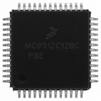
MC9S12C128CPBE Freescale Semiconductor, MC9S12C128CPBE Datasheet - Page 331

MC9S12C128CPBE
Manufacturer Part Number
MC9S12C128CPBE
Description
IC MCU 128K FLASH 25MHZ 52-LQFP
Manufacturer
Freescale Semiconductor
Series
HCS12r
Specifications of MC9S12C128CPBE
Core Processor
HCS12
Core Size
16-Bit
Speed
25MHz
Connectivity
CAN, EBI/EMI, SCI, SPI
Peripherals
POR, PWM, WDT
Number Of I /o
35
Program Memory Size
128KB (128K x 8)
Program Memory Type
FLASH
Ram Size
4K x 8
Voltage - Supply (vcc/vdd)
2.35 V ~ 5.5 V
Data Converters
A/D 8x10b
Oscillator Type
Internal
Operating Temperature
-40°C ~ 85°C
Package / Case
52-LQFP
Lead Free Status / RoHS Status
Lead free / RoHS Compliant
Eeprom Size
-
Available stocks
Company
Part Number
Manufacturer
Quantity
Price
Company:
Part Number:
MC9S12C128CPBE
Manufacturer:
Freescale Semiconductor
Quantity:
10 000
Company:
Part Number:
MC9S12C128CPBER
Manufacturer:
Freescale Semiconductor
Quantity:
10 000
- Current page: 331 of 690
- Download datasheet (4Mb)
10.4.3.1
The MSCAN protects the user from accidentally violating the CAN protocol through programming errors.
The protection logic implements the following features:
10.4.3.2
Figure 10-42
The clock source bit (CLKSRC) in the CANCTL1 register (10.3.2.2/10-294) defines whether the internal
CANCLK is connected to the output of a crystal oscillator (oscillator clock) or to the bus clock.
The clock source has to be chosen such that the tight oscillator tolerance requirements (up to 0.4%) of the
CAN protocol are met. Additionally, for high CAN bus rates (1 Mbps), a 45% to 55% duty cycle of the
clock is required.
Freescale Semiconductor
•
•
•
•
The receive and transmit error counters cannot be written or otherwise manipulated.
All registers which control the configuration of the MSCAN cannot be modified while the MSCAN
is on-line. The MSCAN has to be in Initialization Mode. The corresponding INITRQ/INITAK
handshake bits in the CANCTL0/CANCTL1 registers (see
Register 0
— MSCAN control 1 register (CANCTL1)
— MSCAN bus timing registers 0 and 1 (CANBTR0, CANBTR1)
— MSCAN identifier acceptance control register (CANIDAC)
— MSCAN identifier acceptance registers (CANIDAR0–CANIDAR7)
— MSCAN identifier mask registers (CANIDMR0–CANIDMR7)
The TXCAN pin is immediately forced to a recessive state when the MSCAN goes into the power
down mode or initialization mode (see
Section 10.4.5.5, “MSCAN Initialization
The MSCAN enable bit (CANE) is writable only once in normal system operation modes, which
provides further protection against inadvertently disabling the MSCAN.
Oscillator Clock
Bus Clock
Protocol Violation Protection
Clock System
shows the structure of the MSCAN clock generation circuitry.
(CANCTL0)”) serve as a lock to protect the following registers:
Figure 10-42. MSCAN Clocking Scheme
MC9S12C-Family / MC9S12GC-Family
CLKSRC
Section 10.4.5.6, “MSCAN Power Down
Chapter 10 Freescale’s Scalable Controller Area Network (S12MSCANV2)
Rev 01.24
Mode”).
CANCLK
MSCAN
CLKSRC
Prescaler
(1 .. 64)
Section 10.3.2.1, “MSCAN Control
Time quanta clock (Tq)
Mode,” and
331
Related parts for MC9S12C128CPBE
Image
Part Number
Description
Manufacturer
Datasheet
Request
R
Part Number:
Description:
Manufacturer:
Freescale Semiconductor, Inc
Datasheet:
Part Number:
Description:
Manufacturer:
Freescale Semiconductor, Inc
Datasheet:
Part Number:
Description:
Manufacturer:
Freescale Semiconductor, Inc
Datasheet:
Part Number:
Description:
Manufacturer:
Freescale Semiconductor, Inc
Datasheet:
Part Number:
Description:
Manufacturer:
Freescale Semiconductor, Inc
Datasheet:
Part Number:
Description:
Manufacturer:
Freescale Semiconductor, Inc
Datasheet:
Part Number:
Description:
Manufacturer:
Freescale Semiconductor, Inc
Datasheet:
Part Number:
Description:
Manufacturer:
Freescale Semiconductor, Inc
Datasheet:
Part Number:
Description:
Manufacturer:
Freescale Semiconductor, Inc
Datasheet:
Part Number:
Description:
Manufacturer:
Freescale Semiconductor, Inc
Datasheet:
Part Number:
Description:
Manufacturer:
Freescale Semiconductor, Inc
Datasheet:
Part Number:
Description:
Manufacturer:
Freescale Semiconductor, Inc
Datasheet:
Part Number:
Description:
Manufacturer:
Freescale Semiconductor, Inc
Datasheet:
Part Number:
Description:
Manufacturer:
Freescale Semiconductor, Inc
Datasheet:
Part Number:
Description:
Manufacturer:
Freescale Semiconductor, Inc
Datasheet:


