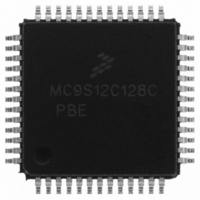
MC9S12C128CPBE Freescale Semiconductor, MC9S12C128CPBE Datasheet - Page 17

MC9S12C128CPBE
Manufacturer Part Number
MC9S12C128CPBE
Description
IC MCU 128K FLASH 25MHZ 52-LQFP
Manufacturer
Freescale Semiconductor
Series
HCS12r
Specifications of MC9S12C128CPBE
Core Processor
HCS12
Core Size
16-Bit
Speed
25MHz
Connectivity
CAN, EBI/EMI, SCI, SPI
Peripherals
POR, PWM, WDT
Number Of I /o
35
Program Memory Size
128KB (128K x 8)
Program Memory Type
FLASH
Ram Size
4K x 8
Voltage - Supply (vcc/vdd)
2.35 V ~ 5.5 V
Data Converters
A/D 8x10b
Oscillator Type
Internal
Operating Temperature
-40°C ~ 85°C
Package / Case
52-LQFP
Lead Free Status / RoHS Status
Lead free / RoHS Compliant
Eeprom Size
-
Available stocks
Company
Part Number
Manufacturer
Quantity
Price
Company:
Part Number:
MC9S12C128CPBE
Manufacturer:
Freescale Semiconductor
Quantity:
10 000
Company:
Part Number:
MC9S12C128CPBER
Manufacturer:
Freescale Semiconductor
Quantity:
10 000
- Current page: 17 of 690
- Download datasheet (4Mb)
Chapter 1
MC9S12C and MC9S12GC Device Overview (MC9S12C128)
1.1
The MC9S12C-Family / MC9S12GC-Family are 48/52/80 pin Flash-based MCU families, which deliver
the power and flexibility of the 16-bit core to a whole new range of cost and space sensitive, general
purpose industrial and automotive network applications. All MC9S12C-Family / MC9S12GC-Family
members feature standard on-chip peripherals including a 16-bit central processing unit (CPU12), up to
128K bytes of Flash EEPROM, up to 4K bytes of RAM, an asynchronous serial communications interface
(SCI), a serial peripheral interface (SPI), an 8-channel 16-bit timer module (TIM), a 6-channel 8-bit pulse
width modulator (PWM), an 8-channel, 10-bit analog-to-digital converter (ADC).
The MC9S12C128-Family members also feature a CAN 2.0 A, B software compatible module
(MSCAN12).
All MC9S12C-Family / MC9S12GC-Family devices feature full 16-bit data paths throughout. The
inclusion of a PLL circuit allows power consumption and performance to be adjusted to suit operational
requirements. In addition to the I/O ports available in each module, up to 10 dedicated I/O port bits are
available with wake-up capability from stop or wait mode. The devices are available in 48-, 52-, and 80-
pin QFP packages, with the 80-pin version pin compatible to the HCS12 A, B, and D Family derivatives.
1.1.1
Freescale Semiconductor
•
•
16-bit HCS12 core:
— HCS12 CPU
— MMC (memory map and interface)
— INT (interrupt control)
— BDM (background debug mode)
— DBG12 (enhanced debug12 module, including breakpoints and change-of-flow trace buffer)
— MEBI (multiplexed expansion bus interface) available only in 80-pin package version
Wake-up interrupt inputs:
— Up to 12 port bits available for wake up interrupt function with digital filtering
Introduction
– Upward compatible with M68HC11 instruction set
– Interrupt stacking and programmer’s model identical to M68HC11
– Instruction queue
– Enhanced indexed addressing
Features
MC9S12C-Family / MC9S12GC-Family
Rev 01.24
17
Related parts for MC9S12C128CPBE
Image
Part Number
Description
Manufacturer
Datasheet
Request
R
Part Number:
Description:
Manufacturer:
Freescale Semiconductor, Inc
Datasheet:
Part Number:
Description:
Manufacturer:
Freescale Semiconductor, Inc
Datasheet:
Part Number:
Description:
Manufacturer:
Freescale Semiconductor, Inc
Datasheet:
Part Number:
Description:
Manufacturer:
Freescale Semiconductor, Inc
Datasheet:
Part Number:
Description:
Manufacturer:
Freescale Semiconductor, Inc
Datasheet:
Part Number:
Description:
Manufacturer:
Freescale Semiconductor, Inc
Datasheet:
Part Number:
Description:
Manufacturer:
Freescale Semiconductor, Inc
Datasheet:
Part Number:
Description:
Manufacturer:
Freescale Semiconductor, Inc
Datasheet:
Part Number:
Description:
Manufacturer:
Freescale Semiconductor, Inc
Datasheet:
Part Number:
Description:
Manufacturer:
Freescale Semiconductor, Inc
Datasheet:
Part Number:
Description:
Manufacturer:
Freescale Semiconductor, Inc
Datasheet:
Part Number:
Description:
Manufacturer:
Freescale Semiconductor, Inc
Datasheet:
Part Number:
Description:
Manufacturer:
Freescale Semiconductor, Inc
Datasheet:
Part Number:
Description:
Manufacturer:
Freescale Semiconductor, Inc
Datasheet:
Part Number:
Description:
Manufacturer:
Freescale Semiconductor, Inc
Datasheet:


