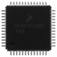
MC9S12C128CPBE Freescale Semiconductor, MC9S12C128CPBE Datasheet - Page 137

MC9S12C128CPBE
Manufacturer Part Number
MC9S12C128CPBE
Description
IC MCU 128K FLASH 25MHZ 52-LQFP
Manufacturer
Freescale Semiconductor
Series
HCS12r
Specifications of MC9S12C128CPBE
Core Processor
HCS12
Core Size
16-Bit
Speed
25MHz
Connectivity
CAN, EBI/EMI, SCI, SPI
Peripherals
POR, PWM, WDT
Number Of I /o
35
Program Memory Size
128KB (128K x 8)
Program Memory Type
FLASH
Ram Size
4K x 8
Voltage - Supply (vcc/vdd)
2.35 V ~ 5.5 V
Data Converters
A/D 8x10b
Oscillator Type
Internal
Operating Temperature
-40°C ~ 85°C
Package / Case
52-LQFP
Lead Free Status / RoHS Status
Lead free / RoHS Compliant
Eeprom Size
-
Available stocks
Company
Part Number
Manufacturer
Quantity
Price
Company:
Part Number:
MC9S12C128CPBE
Manufacturer:
Freescale Semiconductor
Quantity:
10 000
Company:
Part Number:
MC9S12C128CPBER
Manufacturer:
Freescale Semiconductor
Quantity:
10 000
- Current page: 137 of 690
- Download datasheet (4Mb)
4.3.2.4
Read: Anytime when register is in the map
Write: Anytime when register is in the map
This register controls the data direction for port B. When port B is operating as a general-purpose I/O port,
DDRB determines the primary direction for each port B pin. A 1 causes the associated port pin to be an
output and a 0 causes the associated pin to be a high-impedance input. The value in a DDR bit also affects
the source of data for reads of the corresponding PORTB register. If the DDR bit is 0 (input) the buffered
pin input state is read. If the DDR bit is 1 (output) the associated port data register bit state is read.
This register is not in the on-chip memory map in expanded and special peripheral modes. Therefore, these
accesses will be echoed externally. It is reset to 0x00 so the DDR does not override the three-state control
signals.
Freescale Semiconductor
Module Base + 0x0003
Starting address location affected by INITRG register setting.
Reset
DDRB
Field
7:0
W
R
Bit 7
Data Direction Port B
0 Configure the corresponding I/O pin as an input
1 Configure the corresponding I/O pin as an output
Data Direction Register B (DDRB)
0
7
6
0
6
Figure 4-5. Data Direction Register B (DDRB)
Table 4-4. DDRB Field Descriptions
MC9S12C-Family / MC9S12GC-Family
5
0
5
Rev 01.24
4
0
4
Description
Chapter 4 Multiplexed External Bus Interface (MEBIV3)
3
0
3
2
0
2
1
0
1
Bit 0
0
0
137
Related parts for MC9S12C128CPBE
Image
Part Number
Description
Manufacturer
Datasheet
Request
R
Part Number:
Description:
Manufacturer:
Freescale Semiconductor, Inc
Datasheet:
Part Number:
Description:
Manufacturer:
Freescale Semiconductor, Inc
Datasheet:
Part Number:
Description:
Manufacturer:
Freescale Semiconductor, Inc
Datasheet:
Part Number:
Description:
Manufacturer:
Freescale Semiconductor, Inc
Datasheet:
Part Number:
Description:
Manufacturer:
Freescale Semiconductor, Inc
Datasheet:
Part Number:
Description:
Manufacturer:
Freescale Semiconductor, Inc
Datasheet:
Part Number:
Description:
Manufacturer:
Freescale Semiconductor, Inc
Datasheet:
Part Number:
Description:
Manufacturer:
Freescale Semiconductor, Inc
Datasheet:
Part Number:
Description:
Manufacturer:
Freescale Semiconductor, Inc
Datasheet:
Part Number:
Description:
Manufacturer:
Freescale Semiconductor, Inc
Datasheet:
Part Number:
Description:
Manufacturer:
Freescale Semiconductor, Inc
Datasheet:
Part Number:
Description:
Manufacturer:
Freescale Semiconductor, Inc
Datasheet:
Part Number:
Description:
Manufacturer:
Freescale Semiconductor, Inc
Datasheet:
Part Number:
Description:
Manufacturer:
Freescale Semiconductor, Inc
Datasheet:
Part Number:
Description:
Manufacturer:
Freescale Semiconductor, Inc
Datasheet:


