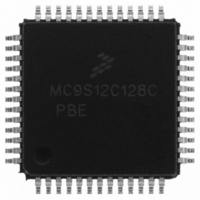
MC9S12C128CPBE Freescale Semiconductor, MC9S12C128CPBE Datasheet - Page 505

MC9S12C128CPBE
Manufacturer Part Number
MC9S12C128CPBE
Description
IC MCU 128K FLASH 25MHZ 52-LQFP
Manufacturer
Freescale Semiconductor
Series
HCS12r
Specifications of MC9S12C128CPBE
Core Processor
HCS12
Core Size
16-Bit
Speed
25MHz
Connectivity
CAN, EBI/EMI, SCI, SPI
Peripherals
POR, PWM, WDT
Number Of I /o
35
Program Memory Size
128KB (128K x 8)
Program Memory Type
FLASH
Ram Size
4K x 8
Voltage - Supply (vcc/vdd)
2.35 V ~ 5.5 V
Data Converters
A/D 8x10b
Oscillator Type
Internal
Operating Temperature
-40°C ~ 85°C
Package / Case
52-LQFP
Lead Free Status / RoHS Status
Lead free / RoHS Compliant
Eeprom Size
-
Available stocks
Company
Part Number
Manufacturer
Quantity
Price
Company:
Part Number:
MC9S12C128CPBE
Manufacturer:
Freescale Semiconductor
Quantity:
10 000
Company:
Part Number:
MC9S12C128CPBER
Manufacturer:
Freescale Semiconductor
Quantity:
10 000
- Current page: 505 of 690
- Download datasheet (4Mb)
18.3
This section describes the
18.3.1
The
addresses between
HCS12 Core PPAGE register is used to map the logical
0xBFFF to
18.3.2.5) can be set to globally protect the entire Flash
Flash array starting address (called lower) towards higher addresses,
Flash array end address
Flash array addresses covered by these protectable regions are shown in Figure 18-2.
area is mainly targeted to hold the boot loader code since it covers the vector space.
can be used for EEPROM emulation in an MCU without an EEPROM module since it can be left
unprotected while the remaining addresses are protected from program or erase.
settings as well as security information that allows the MCU to restrict access to the Flash module are
stored in the Flash configuration field described in
1. By placing 0x3E/0x3F in the HCS12 Core PPAGE register, the
Freescale Semiconductor
memory map.
FTS32K
0xFF08–0xFF0C
0xFF00–0xFF07
Memory Map and Registers
Flash Address
any
Module Memory Map
0xFF0D
0xFF0E
0xFF0F
memory map is shown in
physical 16K byte page in the Flash array memory.
0x4000
(called higher), and the remaining addresses, can be activated for
FTS32K
(bytes)
and
Size
8
5
1
1
1
0xFFFF, which corresponds to three 16 Kbyte
Table 18-1. Flash Configuration Field
memory map and registers.
Backdoor Key to unlock security
Reserved
Flash Protection byte
Refer to
Reserved
Flash Security/Options byte
Refer to
MC9S12C-Family / MC9S12GC-Family
Figure
Section 18.3.2.5, “Flash Protection Register (FPROT)”
Section 18.3.2.2, “Flash Security Register (FSEC)”
18-2. The HCS12 architecture places the Flash array
Rev 01.24
Table
bottom/top fixed
array. Three separate areas, one starting from the
middle
18-1.
Description
page ranging from address 0x8000 to
Chapter 18 32 Kbyte Flash Module (S12FTS32KV1)
1
16 Kbyte
The FPROT register (see
one growing downward from the
pages
pages. The content of the
can be seen twice in the MCU
Default protection
The lower address area
The higher address
protection.
Section
The
505
Related parts for MC9S12C128CPBE
Image
Part Number
Description
Manufacturer
Datasheet
Request
R
Part Number:
Description:
Manufacturer:
Freescale Semiconductor, Inc
Datasheet:
Part Number:
Description:
Manufacturer:
Freescale Semiconductor, Inc
Datasheet:
Part Number:
Description:
Manufacturer:
Freescale Semiconductor, Inc
Datasheet:
Part Number:
Description:
Manufacturer:
Freescale Semiconductor, Inc
Datasheet:
Part Number:
Description:
Manufacturer:
Freescale Semiconductor, Inc
Datasheet:
Part Number:
Description:
Manufacturer:
Freescale Semiconductor, Inc
Datasheet:
Part Number:
Description:
Manufacturer:
Freescale Semiconductor, Inc
Datasheet:
Part Number:
Description:
Manufacturer:
Freescale Semiconductor, Inc
Datasheet:
Part Number:
Description:
Manufacturer:
Freescale Semiconductor, Inc
Datasheet:
Part Number:
Description:
Manufacturer:
Freescale Semiconductor, Inc
Datasheet:
Part Number:
Description:
Manufacturer:
Freescale Semiconductor, Inc
Datasheet:
Part Number:
Description:
Manufacturer:
Freescale Semiconductor, Inc
Datasheet:
Part Number:
Description:
Manufacturer:
Freescale Semiconductor, Inc
Datasheet:
Part Number:
Description:
Manufacturer:
Freescale Semiconductor, Inc
Datasheet:
Part Number:
Description:
Manufacturer:
Freescale Semiconductor, Inc
Datasheet:


