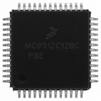
MC9S12C128CPBE Freescale Semiconductor, MC9S12C128CPBE Datasheet - Page 651

MC9S12C128CPBE
Manufacturer Part Number
MC9S12C128CPBE
Description
IC MCU 128K FLASH 25MHZ 52-LQFP
Manufacturer
Freescale Semiconductor
Series
HCS12r
Specifications of MC9S12C128CPBE
Core Processor
HCS12
Core Size
16-Bit
Speed
25MHz
Connectivity
CAN, EBI/EMI, SCI, SPI
Peripherals
POR, PWM, WDT
Number Of I /o
35
Program Memory Size
128KB (128K x 8)
Program Memory Type
FLASH
Ram Size
4K x 8
Voltage - Supply (vcc/vdd)
2.35 V ~ 5.5 V
Data Converters
A/D 8x10b
Oscillator Type
Internal
Operating Temperature
-40°C ~ 85°C
Package / Case
52-LQFP
Lead Free Status / RoHS Status
Lead free / RoHS Compliant
Eeprom Size
-
Available stocks
Company
Part Number
Manufacturer
Quantity
Price
Company:
Part Number:
MC9S12C128CPBE
Manufacturer:
Freescale Semiconductor
Quantity:
10 000
Company:
Part Number:
MC9S12C128CPBER
Manufacturer:
Freescale Semiconductor
Quantity:
10 000
- Current page: 651 of 690
- Download datasheet (4Mb)
A.1.7
This chapter describes the operating conditions of the devices. Unless otherwise noted those conditions
apply to all the following data.
1. The device contains an internal voltage regulator to generate the logic and PLL supply out of the I/O supply. The operating
2. Some blocks e.g. ATD (conversion) and NVMs (program/erase) require higher bus frequencies for proper operation.
3. Some blocks e.g. ATD (conversion) and NVMs (program/erase) require higher bus frequencies for proper operation.
Freescale Semiconductor
I/O, Regulator and Analog Supply Voltage
Digital Logic Supply Voltage
PLL Supply Voltage
Voltage Difference V
Voltage Difference V
Bus Frequency
Bus Frequency
Operating Junction Temperature Range
.
conditions apply when this regulator is disabled and the device is powered from an external source.
Using an external regulator, with the internal voltage regulator disabled, an external LVR must be provided.
Operating Conditions
Instead of specifying ambient temperature all parameters are specified for
the more meaningful silicon junction temperature. For power dissipation
calculations refer to
Characteristics”
1
DDX
SSX
to V
to V
Rating
(1)
SSR
DDA
and V
SSA
Section A.1.8, “Power Dissipation and Thermal
MC9S12C-Family / MC9S12GC-Family
Table A-4. Operating Conditions
Rev 01.24
NOTE
Symbol
V
∆
∆
f
f
V
bus
bus
DDPLL
V
VDDX
VSSX
DD5
T
DD
J
(2)
(3)
2.97
2.35
2.35
–0.1
–0.1
0.25
0.25
Min
–40
Appendix A Electrical Characteristics
Typ
2.5
2.5
—
—
—
5
0
0
Max
2.75
2.75
140
5.5
0.1
0.1
25
16
MHz
MHz
Unit
°C
V
V
V
V
V
651
Related parts for MC9S12C128CPBE
Image
Part Number
Description
Manufacturer
Datasheet
Request
R
Part Number:
Description:
Manufacturer:
Freescale Semiconductor, Inc
Datasheet:
Part Number:
Description:
Manufacturer:
Freescale Semiconductor, Inc
Datasheet:
Part Number:
Description:
Manufacturer:
Freescale Semiconductor, Inc
Datasheet:
Part Number:
Description:
Manufacturer:
Freescale Semiconductor, Inc
Datasheet:
Part Number:
Description:
Manufacturer:
Freescale Semiconductor, Inc
Datasheet:
Part Number:
Description:
Manufacturer:
Freescale Semiconductor, Inc
Datasheet:
Part Number:
Description:
Manufacturer:
Freescale Semiconductor, Inc
Datasheet:
Part Number:
Description:
Manufacturer:
Freescale Semiconductor, Inc
Datasheet:
Part Number:
Description:
Manufacturer:
Freescale Semiconductor, Inc
Datasheet:
Part Number:
Description:
Manufacturer:
Freescale Semiconductor, Inc
Datasheet:
Part Number:
Description:
Manufacturer:
Freescale Semiconductor, Inc
Datasheet:
Part Number:
Description:
Manufacturer:
Freescale Semiconductor, Inc
Datasheet:
Part Number:
Description:
Manufacturer:
Freescale Semiconductor, Inc
Datasheet:
Part Number:
Description:
Manufacturer:
Freescale Semiconductor, Inc
Datasheet:
Part Number:
Description:
Manufacturer:
Freescale Semiconductor, Inc
Datasheet:


