MC9S12C128CPBE Freescale Semiconductor, MC9S12C128CPBE Datasheet - Page 198
MC9S12C128CPBE
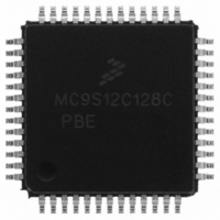
Manufacturer Part Number
MC9S12C128CPBE
Description
IC MCU 128K FLASH 25MHZ 52-LQFP
Manufacturer
Freescale Semiconductor
Series
HCS12r
Specifications of MC9S12C128CPBE
Core Processor
HCS12
Core Size
16-Bit
Speed
25MHz
Connectivity
CAN, EBI/EMI, SCI, SPI
Peripherals
POR, PWM, WDT
Number Of I /o
35
Program Memory Size
128KB (128K x 8)
Program Memory Type
FLASH
Ram Size
4K x 8
Voltage - Supply (vcc/vdd)
2.35 V ~ 5.5 V
Data Converters
A/D 8x10b
Oscillator Type
Internal
Operating Temperature
-40°C ~ 85°C
Package / Case
52-LQFP
Lead Free Status / RoHS Status
Lead free / RoHS Compliant
Eeprom Size
-
Available stocks
Company
Part Number
Manufacturer
Quantity
Price

Company:
Part Number:
MC9S12C128CPBE
Manufacturer:
Freescale Semiconductor
Quantity:
10 000
Company:
Part Number:
MC9S12C128CPBER
Manufacturer:
Freescale Semiconductor
Quantity:
10 000


Chapter 7 Debug Module (DBGV1) Block Description
1. The DBG module is designed for backwards compatibility to existing BKP modules. Register and bit names have changed from
2. Comparator C can be used to enhance the BKP mode by providing a third breakpoint.
7.3.2.1
198
Module Base + 0x0020
Starting address location affected by INITRG register setting.
the BKP module. This column shows the DBG register name, as well as the BKP register name for reference.
TRGSEL
DBGEN
Reset
BEGIN
Field
ARM
7
6
5
4
W
R
DBGEN
DBG Mode Enable Bit — The DBGEN bit enables the DBG module for use in DBG mode. This bit cannot be
set if the MCU is in secure mode.
0 DBG mode disabled
1 DBG mode enabled
Arm Bit — The ARM bit controls whether the debugger is comparing and storing data in the trace buffer. See
Section 7.4.2.4, “Arming the DBG
0 Debugger unarmed
1 Debugger armed
Note: This bit cannot be set if the DBGEN bit is not also being set at the same time. For example, a write of 01
Trigger Selection Bit — The TRGSEL bit controls the triggering condition for comparators A and B in DBG
mode. It serves essentially the same function as the TAGAB bit in the DBGC2 register does in BKP mode. See
Section 7.4.2.1.2, “Trigger
based on comparator A and B if enabled in DBG mode (DBGBRK = 1). Please refer to
“Breakpoint Based on Comparator A and
0 Trigger on any compare address match
1 Trigger before opcode at compare address gets executed (tagged-type)
Begin/End Trigger Bit — The BEGIN bit controls whether the trigger begins or ends storing of data in the trace
buffer. See
more details.
0 Trigger at end of stored data
1 Trigger before storing data
Debug Control Register 1 (DBGC1)
0
7
All bits are used in DBG mode only.
This register cannot be written if BKP mode is enabled (BKABEN in
DBGC2 is set).
to DBGEN[7:6] will be interpreted as a write of 00.
= Unimplemented or Reserved
Section 7.4.2.8.1, “Storing with
ARM
0
6
Figure 7-4. Debug Control Register (DBGC1)
Table 7-3. DBGC1 Field Descriptions
Selection,” for more information. TRGSEL may also determine the type of breakpoint
TRGSEL
MC9S12C-Family / MC9S12GC-Family
0
5
Module,” for more information.
B.”
BEGIN
Begin-Trigger,” and
Rev 01.24
NOTE
NOTE
0
4
Description
DBGBRK
0
3
Section 7.4.2.8.2, “Storing with
0
0
2
Freescale Semiconductor
Section 7.4.3.1,
0
1
CAPMOD
End-Trigger,” for
0
0
Related parts for MC9S12C128CPBE
Image
Part Number
Description
Manufacturer
Datasheet
Request
R

Part Number:
Description:
Manufacturer:
Freescale Semiconductor, Inc
Datasheet:
Part Number:
Description:
Manufacturer:
Freescale Semiconductor, Inc
Datasheet:
Part Number:
Description:
Manufacturer:
Freescale Semiconductor, Inc
Datasheet:
Part Number:
Description:
Manufacturer:
Freescale Semiconductor, Inc
Datasheet:
Part Number:
Description:
Manufacturer:
Freescale Semiconductor, Inc
Datasheet:
Part Number:
Description:
Manufacturer:
Freescale Semiconductor, Inc
Datasheet:
Part Number:
Description:
Manufacturer:
Freescale Semiconductor, Inc
Datasheet:
Part Number:
Description:
Manufacturer:
Freescale Semiconductor, Inc
Datasheet:
Part Number:
Description:
Manufacturer:
Freescale Semiconductor, Inc
Datasheet:
Part Number:
Description:
Manufacturer:
Freescale Semiconductor, Inc
Datasheet:
Part Number:
Description:
Manufacturer:
Freescale Semiconductor, Inc
Datasheet:
Part Number:
Description:
Manufacturer:
Freescale Semiconductor, Inc
Datasheet:
Part Number:
Description:
Manufacturer:
Freescale Semiconductor, Inc
Datasheet:
Part Number:
Description:
Manufacturer:
Freescale Semiconductor, Inc
Datasheet:
Part Number:
Description:
Manufacturer:
Freescale Semiconductor, Inc
Datasheet: