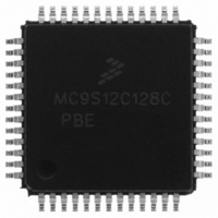
MC9S12C128CPBE Freescale Semiconductor, MC9S12C128CPBE Datasheet - Page 371

MC9S12C128CPBE
Manufacturer Part Number
MC9S12C128CPBE
Description
IC MCU 128K FLASH 25MHZ 52-LQFP
Manufacturer
Freescale Semiconductor
Series
HCS12r
Specifications of MC9S12C128CPBE
Core Processor
HCS12
Core Size
16-Bit
Speed
25MHz
Connectivity
CAN, EBI/EMI, SCI, SPI
Peripherals
POR, PWM, WDT
Number Of I /o
35
Program Memory Size
128KB (128K x 8)
Program Memory Type
FLASH
Ram Size
4K x 8
Voltage - Supply (vcc/vdd)
2.35 V ~ 5.5 V
Data Converters
A/D 8x10b
Oscillator Type
Internal
Operating Temperature
-40°C ~ 85°C
Package / Case
52-LQFP
Lead Free Status / RoHS Status
Lead free / RoHS Compliant
Eeprom Size
-
Available stocks
Company
Part Number
Manufacturer
Quantity
Price
Company:
Part Number:
MC9S12C128CPBE
Manufacturer:
Freescale Semiconductor
Quantity:
10 000
Company:
Part Number:
MC9S12C128CPBER
Manufacturer:
Freescale Semiconductor
Quantity:
10 000
- Current page: 371 of 690
- Download datasheet (4Mb)
Chapter 12 Pulse-Width Modulator (PWM8B6CV1) Block Description
12.4
Functional Description
12.4.1
PWM Clock Select
There are four available clocks called clock A, clock B, clock SA (scaled A), and clock SB (scaled B).
These four clocks are based on the bus clock.
Clock A and B can be software selected to be 1, 1/2, 1/4, 1/8,..., 1/64, 1/128 times the bus clock. Clock SA
uses clock A as an input and divides it further with a reloadable counter. Similarly, clock SB uses clock B
as an input and divides it further with a reloadable counter. The rates available for clock SA are software
selectable to be clock A divided by 2, 4, 6, 8, ..., or 512 in increments of divide by 2. Similar rates are
available for clock SB. Each PWM channel has the capability of selecting one of two clocks, either the
pre-scaled clock (clock A or B) or the scaled clock (clock SA or SB).
The block diagram in
Figure 12-34
shows the four different clocks and how the scaled clocks are created.
12.4.1.1
Prescale
The input clock to the PWM prescaler is the bus clock. It can be disabled whenever the part is in freeze
mode by setting the PFRZ bit in the PWMCTL register. If this bit is set, whenever the MCU is in freeze
mode the input clock to the prescaler is disabled. This is useful for emulation in order to freeze the PWM.
The input clock can also be disabled when all six PWM channels are disabled (PWME5–PWME0 = 0)
This is useful for reducing power by disabling the prescale counter.
Clock A and clock B are scaled values of the input clock. The value is software selectable for both clock A
and clock B and has options of 1, 1/2, 1/4, 1/8, 1/16, 1/32, 1/64, or 1/128 times the bus clock. The value
selected for clock A is determined by the PCKA2, PCKA1, and PCKA0 bits in the PWMPRCLK register.
The value selected for clock B is determined by the PCKB2, PCKB1, and PCKB0 bits also in the
PWMPRCLK register.
Freescale Semiconductor
MC9S12C-Family / MC9S12GC-Family
371
Rev 01.24
Related parts for MC9S12C128CPBE
Image
Part Number
Description
Manufacturer
Datasheet
Request
R
Part Number:
Description:
Manufacturer:
Freescale Semiconductor, Inc
Datasheet:
Part Number:
Description:
Manufacturer:
Freescale Semiconductor, Inc
Datasheet:
Part Number:
Description:
Manufacturer:
Freescale Semiconductor, Inc
Datasheet:
Part Number:
Description:
Manufacturer:
Freescale Semiconductor, Inc
Datasheet:
Part Number:
Description:
Manufacturer:
Freescale Semiconductor, Inc
Datasheet:
Part Number:
Description:
Manufacturer:
Freescale Semiconductor, Inc
Datasheet:
Part Number:
Description:
Manufacturer:
Freescale Semiconductor, Inc
Datasheet:
Part Number:
Description:
Manufacturer:
Freescale Semiconductor, Inc
Datasheet:
Part Number:
Description:
Manufacturer:
Freescale Semiconductor, Inc
Datasheet:
Part Number:
Description:
Manufacturer:
Freescale Semiconductor, Inc
Datasheet:
Part Number:
Description:
Manufacturer:
Freescale Semiconductor, Inc
Datasheet:
Part Number:
Description:
Manufacturer:
Freescale Semiconductor, Inc
Datasheet:
Part Number:
Description:
Manufacturer:
Freescale Semiconductor, Inc
Datasheet:
Part Number:
Description:
Manufacturer:
Freescale Semiconductor, Inc
Datasheet:
Part Number:
Description:
Manufacturer:
Freescale Semiconductor, Inc
Datasheet:


