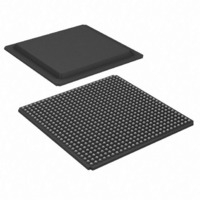
XC2V2000-4FGG676C Xilinx Inc, XC2V2000-4FGG676C Datasheet - Page 12

XC2V2000-4FGG676C
Manufacturer Part Number
XC2V2000-4FGG676C
Description
FPGA Virtex-II™ Family 2M Gates 24192 Cells 650MHz 0.15um/0.12um (CMOS) Technology 1.5V 676-Pin FBGA
Manufacturer
Xilinx Inc
Series
Virtex™-IIr
Datasheet
1.XC2V250-4FGG256C.pdf
(318 pages)
Specifications of XC2V2000-4FGG676C
Package
676FBGA
Family Name
Virtex-IIÂ
Device Logic Units
24192
Device System Gates
2000000
Number Of Registers
21504
Maximum Internal Frequency
650 MHz
Typical Operating Supply Voltage
1.5 V
Maximum Number Of User I/os
456
Ram Bits
1032192
Number Of Labs/clbs
2688
Total Ram Bits
1032192
Number Of I /o
456
Number Of Gates
2000000
Voltage - Supply
1.425 V ~ 1.575 V
Mounting Type
Surface Mount
Operating Temperature
0°C ~ 85°C
Package / Case
676-BBGA
Lead Free Status / RoHS Status
Lead free / RoHS Compliant
Number Of Logic Elements/cells
-
Lead Free Status / RoHS Status
Lead free / RoHS Compliant
Other names
122-1351
Available stocks
Company
Part Number
Manufacturer
Quantity
Price
Company:
Part Number:
XC2V2000-4FGG676C
Manufacturer:
Xilinx Inc
Quantity:
10 000
- Current page: 12 of 318
- Download datasheet (3Mb)
DS031-2 (v3.5) November 5, 2007
Product Specification
Figure 5: LVTTL, LVCMOS or PCI SelectI/O-Ultra
Program
Delay
OBUF
R
registers
Shared
Program
Current
by all
(O/T) CLK1
(O/T) CLK2
V CCO
IBUF
(O/T) CE
V CCO
(O/T) 1
(O/T) 2
REV
SR
Standards
Clamp
Diode
Figure 4: Register / Latch Configuration in an IOB Block
V CCO
10KΩ –
10KΩ –
60KΩ
60KΩ
Keeper
Weak
V CCAUX = 3.3V
V CCINT = 1.5V
DS031_23_022205
D1
CE
CK1
D2
CE
CK2
SR REV
SR REV
www.xilinx.com
FF
LATCH
FF
LATCH
PAD
Q1
Q2
Attribute INIT1
Attribute INIT1
Input/Output Individual Options
Each device pad has optional pull-up and pull-down in all
SelectI/O-Ultra configurations. Each device pad has
optional weak-keeper in LVTTL, LVCMOS, and PCI
SelectI/O-Ultra configurations, as illustrated in
Values of the optional pull-up and pull-down resistors are in
the range 10 - 60 KΩ, which is the specification for V
when operating at 3.3V (from 3.0 to 3.6V only). The clamp
diode is always present, even when power is not.
The optional weak-keeper circuit is connected to each user
I/O pad. When selected, the circuit monitors the voltage on
the pad and weakly drives the pin High or Low. If the pin is
connected to a multiple-source signal, the weak-keeper
holds the signal in its last state if all drivers are disabled.
Maintaining a valid logic level in this way eliminates bus
chatter. An enabled pull-up or pull-down overrides the
weak-keeper circuit.
LVTTL sinks and sources current up to 24 mA. The current
is programmable for LVTTL and LVCMOS SelectI/O-Ultra
standards (see
trols for each output driver, minimize bus transients. For
LVDCI and LVDCI_DV2 standards, drive strength and
slew-rate controls are not available.
DDR MUX
FF1
FF2
Virtex-II Platform FPGAs: Functional Description
INIT0
SRHIGH
SRLOW
INIT0
SRHIGH
SRLOW
Table
4). Drive-strength and slew-rate con-
Reset Type
SYNC
ASYNC
DS031_25_110300
(OQ or TQ)
Module 2 of 4
Figure
CCO
5.
4
Related parts for XC2V2000-4FGG676C
Image
Part Number
Description
Manufacturer
Datasheet
Request
R

Part Number:
Description:
IC VIRTEX-II FPGA 2M 896-FCBGA
Manufacturer:
Xilinx Inc
Datasheet:

Part Number:
Description:
IC FPGA VIRTEX-II 2M 575-MBGA
Manufacturer:
Xilinx Inc
Datasheet:

Part Number:
Description:
IC FPGA VIRTEX-II 2M 676-FBGA
Manufacturer:
Xilinx Inc
Datasheet:

Part Number:
Description:
IC FPGA VIRTEX-II 2M 676-FBGA
Manufacturer:
Xilinx Inc
Datasheet:

Part Number:
Description:
IC FPGA VIRTEX-II 2M 575-MBGA
Manufacturer:
Xilinx Inc
Datasheet:

Part Number:
Description:
IC FPGA VIRTEX-II 2M 575-MBGA
Manufacturer:
Xilinx Inc
Datasheet:

Part Number:
Description:
IC FPGA VIRTEX-II 2M 896-FBGA
Manufacturer:
Xilinx Inc
Datasheet:

Part Number:
Description:
IC FPGA VIRTEX-II 2M 896-FBGA
Manufacturer:
Xilinx Inc
Datasheet:

Part Number:
Description:
IC FPGA VIRTEX-II 2M 676-FBGA
Manufacturer:
Xilinx Inc
Datasheet:

Part Number:
Description:
IC FPGA VIRTEX-II 2M 676-FBGA
Manufacturer:
Xilinx Inc
Datasheet:

Part Number:
Description:
IC FPGA VIRTEX-II 2M 575-MBGA
Manufacturer:
Xilinx Inc
Datasheet:

Part Number:
Description:
IC FPGA VIRTEX-II 2M 575-MBGA
Manufacturer:
Xilinx Inc
Datasheet:

Part Number:
Description:
IC FPGA VIRTEX-II 2M 896-FBGA
Manufacturer:
Xilinx Inc
Datasheet:

Part Number:
Description:
IC FPGA VIRTEX-II 575PBGA
Manufacturer:
Xilinx Inc
Datasheet:

Part Number:
Description:
IC FPGA VIRTEX-II 896FCBGA
Manufacturer:
Xilinx Inc
Datasheet:


