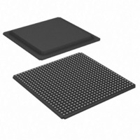
XC2V2000-4FGG676C Xilinx Inc, XC2V2000-4FGG676C Datasheet - Page 51

XC2V2000-4FGG676C
Manufacturer Part Number
XC2V2000-4FGG676C
Description
FPGA Virtex-II™ Family 2M Gates 24192 Cells 650MHz 0.15um/0.12um (CMOS) Technology 1.5V 676-Pin FBGA
Manufacturer
Xilinx Inc
Series
Virtex™-IIr
Datasheet
1.XC2V250-4FGG256C.pdf
(318 pages)
Specifications of XC2V2000-4FGG676C
Package
676FBGA
Family Name
Virtex-IIÂ
Device Logic Units
24192
Device System Gates
2000000
Number Of Registers
21504
Maximum Internal Frequency
650 MHz
Typical Operating Supply Voltage
1.5 V
Maximum Number Of User I/os
456
Ram Bits
1032192
Number Of Labs/clbs
2688
Total Ram Bits
1032192
Number Of I /o
456
Number Of Gates
2000000
Voltage - Supply
1.425 V ~ 1.575 V
Mounting Type
Surface Mount
Operating Temperature
0°C ~ 85°C
Package / Case
676-BBGA
Lead Free Status / RoHS Status
Lead free / RoHS Compliant
Number Of Logic Elements/cells
-
Lead Free Status / RoHS Status
Lead free / RoHS Compliant
Other names
122-1351
Available stocks
Company
Part Number
Manufacturer
Quantity
Price
Company:
Part Number:
XC2V2000-4FGG676C
Manufacturer:
Xilinx Inc
Quantity:
10 000
- Current page: 51 of 318
- Download datasheet (3Mb)
Table 4: Quiescent Supply Current
Power-On Power Supply Requirements
Xilinx FPGAs require a certain amount of supply current
during power-on to insure proper device operation. The
actual current consumed depends on the power-on ramp
rate of the power supply.
The V
ramp on, monotonically, no faster than 200 μs and no slower
than 50 ms. Ramp on is defined as: 0 V
ply voltages.
Table 5
devices for proper power on and configuration.
Power supplies can be turned on in any sequence.
DS031-3 (v3.5) November 5, 2007
Product Specification
Notes:
1. With no output current loads, no active input pull-up resistors, all I/O pins are 3-state and floating.
2. If DCI or differential signaling is used, more accurate values can be obtained by using the Power Estimator or XPOWER™.
3. Data are retained even if V
4. Values specified for quiescent supply current parameters are Commercial Grade. For Industrial Grade values, multiply Commercial
I
Symbol
I
CCAUXQ
CCINTQ
I
CCOQ
Grade values by 1.25.
CCINT
shows the minimum current required by Virtex-II
, V
R
Quiescent V
Quiescent V
Quiescent V
CCAUX
, and V
CCINT
CCO
CCAUX
Description
CCO
CCO
supply current
supply current
supply current
drops to 0 V.
power supplies shall each
DC
to minimum sup-
(1,2)
(1,2)
(1)
www.xilinx.com
Virtex-II Platform FPGAs: DC and Switching Characteristics
XC2V1000
XC2V1500
XC2V2000
XC2V3000
XC2V4000
XC2V6000
XC2V8000
XC2V1000
XC2V1500
XC2V2000
XC2V3000
XC2V4000
XC2V6000
XC2V8000
XC2V1000
XC2V1500
XC2V2000
XC2V3000
XC2V4000
XC2V6000
XC2V8000
XC2V250
XC2V500
XC2V250
XC2V500
XC2V250
XC2V500
XC2V40
XC2V80
XC2V40
XC2V80
XC2V40
XC2V80
Device
If any V
draws up to 300 mA, worst case, until the V
up.
to the minimum value above, or larger, the device powers on
properly after all three supplies have passed through their
power-on reset threshold voltages.
Once initialized and configured, use the power calculator to
estimate current drain on these supplies.
Notes:
1. If the V
2. The 300 mA is transient current (peak); it eventually
(2)
be applied before V
damaged if this requirement is violated, but configuration will
probably fail.
disappears even if V
This does not harm the device. If the current is limited
CCO
CCINT
bank powers up before V
Min
ramp rate is longer than 10 ms, then V
CCO
CCAUX
and V
Typical
12.5
12.5
7.5
7.5
does not power up.
10
12
15
20
27
35
45
60
10
10
3
5
8
1
1
1
1
1
2
2
2
2
2
2
5
5
5
5
5
CCAUX
CCAUX
. The device will not be
1100
Max
125
125
150
200
250
350
400
500
650
800
100
100
25
25
25
25
25
50
50
75
75
2
2
2
2
2
4
4
4
4
4
4
, then each bank
CCAUX
Module 3 of 4
CCINT
Units
powers
mA
mA
mA
must
3
Related parts for XC2V2000-4FGG676C
Image
Part Number
Description
Manufacturer
Datasheet
Request
R

Part Number:
Description:
IC VIRTEX-II FPGA 2M 896-FCBGA
Manufacturer:
Xilinx Inc
Datasheet:

Part Number:
Description:
IC FPGA VIRTEX-II 2M 575-MBGA
Manufacturer:
Xilinx Inc
Datasheet:

Part Number:
Description:
IC FPGA VIRTEX-II 2M 676-FBGA
Manufacturer:
Xilinx Inc
Datasheet:

Part Number:
Description:
IC FPGA VIRTEX-II 2M 676-FBGA
Manufacturer:
Xilinx Inc
Datasheet:

Part Number:
Description:
IC FPGA VIRTEX-II 2M 575-MBGA
Manufacturer:
Xilinx Inc
Datasheet:

Part Number:
Description:
IC FPGA VIRTEX-II 2M 575-MBGA
Manufacturer:
Xilinx Inc
Datasheet:

Part Number:
Description:
IC FPGA VIRTEX-II 2M 896-FBGA
Manufacturer:
Xilinx Inc
Datasheet:

Part Number:
Description:
IC FPGA VIRTEX-II 2M 896-FBGA
Manufacturer:
Xilinx Inc
Datasheet:

Part Number:
Description:
IC FPGA VIRTEX-II 2M 676-FBGA
Manufacturer:
Xilinx Inc
Datasheet:

Part Number:
Description:
IC FPGA VIRTEX-II 2M 676-FBGA
Manufacturer:
Xilinx Inc
Datasheet:

Part Number:
Description:
IC FPGA VIRTEX-II 2M 575-MBGA
Manufacturer:
Xilinx Inc
Datasheet:

Part Number:
Description:
IC FPGA VIRTEX-II 2M 575-MBGA
Manufacturer:
Xilinx Inc
Datasheet:

Part Number:
Description:
IC FPGA VIRTEX-II 2M 896-FBGA
Manufacturer:
Xilinx Inc
Datasheet:

Part Number:
Description:
IC FPGA VIRTEX-II 575PBGA
Manufacturer:
Xilinx Inc
Datasheet:

Part Number:
Description:
IC FPGA VIRTEX-II 896FCBGA
Manufacturer:
Xilinx Inc
Datasheet:


