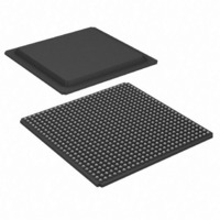
XC2V2000-4FGG676C Xilinx Inc, XC2V2000-4FGG676C Datasheet - Page 96

XC2V2000-4FGG676C
Manufacturer Part Number
XC2V2000-4FGG676C
Description
FPGA Virtex-II™ Family 2M Gates 24192 Cells 650MHz 0.15um/0.12um (CMOS) Technology 1.5V 676-Pin FBGA
Manufacturer
Xilinx Inc
Series
Virtex™-IIr
Datasheet
1.XC2V250-4FGG256C.pdf
(318 pages)
Specifications of XC2V2000-4FGG676C
Package
676FBGA
Family Name
Virtex-IIÂ
Device Logic Units
24192
Device System Gates
2000000
Number Of Registers
21504
Maximum Internal Frequency
650 MHz
Typical Operating Supply Voltage
1.5 V
Maximum Number Of User I/os
456
Ram Bits
1032192
Number Of Labs/clbs
2688
Total Ram Bits
1032192
Number Of I /o
456
Number Of Gates
2000000
Voltage - Supply
1.425 V ~ 1.575 V
Mounting Type
Surface Mount
Operating Temperature
0°C ~ 85°C
Package / Case
676-BBGA
Lead Free Status / RoHS Status
Lead free / RoHS Compliant
Number Of Logic Elements/cells
-
Lead Free Status / RoHS Status
Lead free / RoHS Compliant
Other names
122-1351
Available stocks
Company
Part Number
Manufacturer
Quantity
Price
Company:
Part Number:
XC2V2000-4FGG676C
Manufacturer:
Xilinx Inc
Quantity:
10 000
- Current page: 96 of 318
- Download datasheet (3Mb)
Table 4: Virtex-II Pin Definitions (Continued)
DS031-4 (v3.5) November 5, 2007
Product Specification
Notes:
1. All dedicated pins (JTAG and configuration) are powered by V
PROG_B
DONE
M2, M1, M0
HSWAP_EN
TCK
TDI
TDO
TMS
PWRDWN_B
Other Pins
DXN, DXP
V
RSVD
V
V
V
GND
BATT
CCO
CCAUX
CCINT
Pin Name
R
Input
Input/Output
Input
Input
Input
Input
Output
Input
N/A
Input
N/A
Input
Input
Input
Input
(unsupported)
Direction
Input
Active Low asynchronous reset to configuration logic. This pin has a permanent weak
pull-up resistor.
DONE is a bidirectional signal with an optional internal pull-up resistor. As an output,
this pin indicates completion of the configuration process. As an input, a Low level on
DONE can be configured to delay the start-up sequence.
Configuration mode selection.
Enable I/O pull-ups during configuration.
Boundary Scan Clock.
Boundary Scan Data Input.
Boundary Scan Data Output.
Boundary Scan Mode Select.
Active Low power-down pin (unsupported). Driving this pin Low can adversely affect
device operation and configuration. PWRDWN_B is internally pulled High, which is its
default state. It does not require an external pull-up.
Temperature-sensing diode pins (Anode: DXP, Cathode: DXN).
Decryptor key memory backup supply. Connect V
not used.
Reserved pin - do not connect.
Power-supply pins for the output drivers (per bank).
Power-supply pins for auxiliary circuits.
Power-supply pins for the internal core logic.
Ground.
www.xilinx.com
CCAUX
(independent of the bank V
Description
Virtex-II Platform FPGAs: Pinout Information
BATT
CCO
to V
voltage).
CCAUX
or GND if battery is
Module 4 of 4
4
Related parts for XC2V2000-4FGG676C
Image
Part Number
Description
Manufacturer
Datasheet
Request
R

Part Number:
Description:
IC VIRTEX-II FPGA 2M 896-FCBGA
Manufacturer:
Xilinx Inc
Datasheet:

Part Number:
Description:
IC FPGA VIRTEX-II 2M 575-MBGA
Manufacturer:
Xilinx Inc
Datasheet:

Part Number:
Description:
IC FPGA VIRTEX-II 2M 676-FBGA
Manufacturer:
Xilinx Inc
Datasheet:

Part Number:
Description:
IC FPGA VIRTEX-II 2M 676-FBGA
Manufacturer:
Xilinx Inc
Datasheet:

Part Number:
Description:
IC FPGA VIRTEX-II 2M 575-MBGA
Manufacturer:
Xilinx Inc
Datasheet:

Part Number:
Description:
IC FPGA VIRTEX-II 2M 575-MBGA
Manufacturer:
Xilinx Inc
Datasheet:

Part Number:
Description:
IC FPGA VIRTEX-II 2M 896-FBGA
Manufacturer:
Xilinx Inc
Datasheet:

Part Number:
Description:
IC FPGA VIRTEX-II 2M 896-FBGA
Manufacturer:
Xilinx Inc
Datasheet:

Part Number:
Description:
IC FPGA VIRTEX-II 2M 676-FBGA
Manufacturer:
Xilinx Inc
Datasheet:

Part Number:
Description:
IC FPGA VIRTEX-II 2M 676-FBGA
Manufacturer:
Xilinx Inc
Datasheet:

Part Number:
Description:
IC FPGA VIRTEX-II 2M 575-MBGA
Manufacturer:
Xilinx Inc
Datasheet:

Part Number:
Description:
IC FPGA VIRTEX-II 2M 575-MBGA
Manufacturer:
Xilinx Inc
Datasheet:

Part Number:
Description:
IC FPGA VIRTEX-II 2M 896-FBGA
Manufacturer:
Xilinx Inc
Datasheet:

Part Number:
Description:
IC FPGA VIRTEX-II 575PBGA
Manufacturer:
Xilinx Inc
Datasheet:

Part Number:
Description:
IC FPGA VIRTEX-II 896FCBGA
Manufacturer:
Xilinx Inc
Datasheet:


