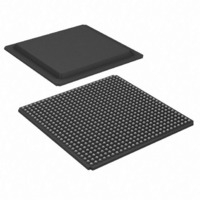
XC2V2000-4FGG676C Xilinx Inc, XC2V2000-4FGG676C Datasheet - Page 54

XC2V2000-4FGG676C
Manufacturer Part Number
XC2V2000-4FGG676C
Description
FPGA Virtex-II™ Family 2M Gates 24192 Cells 650MHz 0.15um/0.12um (CMOS) Technology 1.5V 676-Pin FBGA
Manufacturer
Xilinx Inc
Series
Virtex™-IIr
Datasheet
1.XC2V250-4FGG256C.pdf
(318 pages)
Specifications of XC2V2000-4FGG676C
Package
676FBGA
Family Name
Virtex-IIÂ
Device Logic Units
24192
Device System Gates
2000000
Number Of Registers
21504
Maximum Internal Frequency
650 MHz
Typical Operating Supply Voltage
1.5 V
Maximum Number Of User I/os
456
Ram Bits
1032192
Number Of Labs/clbs
2688
Total Ram Bits
1032192
Number Of I /o
456
Number Of Gates
2000000
Voltage - Supply
1.425 V ~ 1.575 V
Mounting Type
Surface Mount
Operating Temperature
0°C ~ 85°C
Package / Case
676-BBGA
Lead Free Status / RoHS Status
Lead free / RoHS Compliant
Number Of Logic Elements/cells
-
Lead Free Status / RoHS Status
Lead free / RoHS Compliant
Other names
122-1351
Available stocks
Company
Part Number
Manufacturer
Quantity
Price
Company:
Part Number:
XC2V2000-4FGG676C
Manufacturer:
Xilinx Inc
Quantity:
10 000
- Current page: 54 of 318
- Download datasheet (3Mb)
Extended LVDS DC Specifications (LVDSEXT_33 & LVDSEXT_25)
Table 9: Extended LVDS DC Specifications
LVPECL DC Specifications
These values are valid when driving a 100 Ω differential
load only, i.e., a 100 Ω resistor between the two receiver
pins. The V
levels and are compatible with devices tolerant of lower
Table 10: LVPECL DC Specifications
DS031-3 (v3.5) November 5, 2007
Product Specification
Differential output voltage (Q – Q),
Differential input voltage (Q – Q),
Output High voltage for Q and Q
Output Low voltage for Q and Q
Output common-mode voltage
Input common-mode voltage
Q = High (Q – Q), Q = High
Q = High (Q – Q), Q = High
Supply Voltage
DC Parameter
Differential Input Voltage
OH
R
levels are 200 mV below standard LVPECL
DC Parameter
V
V
V
V
CCO
V
OH
OL
IH
IL
Symbol
V
V
V
V
V
V
ODIFF
V
OCM
IDIFF
CCO
ICM
OH
OL
Common-mode input voltage = 1.25 V
Differential input voltage = ±350 mV
R
R
R
R
T
T
T
T
0.96
1.49
0.86
Min
= 100 Ω across Q and Q signals
= 100 Ω across Q and Q signals
= 100 Ω across Q and Q signals
= 100 Ω across Q and Q signals
0.3
1.8
www.xilinx.com
3.0
Virtex-II Platform FPGAs: DC and Switching Characteristics
Conditions
2.125
Max
2.11
1.27
2.72
–
common-mode ranges.
specifications of LVPECL. For more information on using
LVPECL
1.92
1.06
1.49
0.86
,
Min
0.3
see the Virtex-II User Guide.
3.3
2.125
Max
2.28
1.43
2.72
–
0.705
1.125
Min
440
100
0.2
Table 10
3.3 or 2.5
2.13
1.30
1.49
0.86
Min
0.3
1.200
1.25
Typ
350
summarizes the DC output
3.6
2.125
Max
2.41
1.57
2.72
V
–
CCO
1.785
1.375
Max
820
N/A
– 0.5
Module 3 of 4
Units
V
V
V
V
V
V
Units
mV
mV
V
V
V
V
V
6
Related parts for XC2V2000-4FGG676C
Image
Part Number
Description
Manufacturer
Datasheet
Request
R

Part Number:
Description:
IC VIRTEX-II FPGA 2M 896-FCBGA
Manufacturer:
Xilinx Inc
Datasheet:

Part Number:
Description:
IC FPGA VIRTEX-II 2M 575-MBGA
Manufacturer:
Xilinx Inc
Datasheet:

Part Number:
Description:
IC FPGA VIRTEX-II 2M 676-FBGA
Manufacturer:
Xilinx Inc
Datasheet:

Part Number:
Description:
IC FPGA VIRTEX-II 2M 676-FBGA
Manufacturer:
Xilinx Inc
Datasheet:

Part Number:
Description:
IC FPGA VIRTEX-II 2M 575-MBGA
Manufacturer:
Xilinx Inc
Datasheet:

Part Number:
Description:
IC FPGA VIRTEX-II 2M 575-MBGA
Manufacturer:
Xilinx Inc
Datasheet:

Part Number:
Description:
IC FPGA VIRTEX-II 2M 896-FBGA
Manufacturer:
Xilinx Inc
Datasheet:

Part Number:
Description:
IC FPGA VIRTEX-II 2M 896-FBGA
Manufacturer:
Xilinx Inc
Datasheet:

Part Number:
Description:
IC FPGA VIRTEX-II 2M 676-FBGA
Manufacturer:
Xilinx Inc
Datasheet:

Part Number:
Description:
IC FPGA VIRTEX-II 2M 676-FBGA
Manufacturer:
Xilinx Inc
Datasheet:

Part Number:
Description:
IC FPGA VIRTEX-II 2M 575-MBGA
Manufacturer:
Xilinx Inc
Datasheet:

Part Number:
Description:
IC FPGA VIRTEX-II 2M 575-MBGA
Manufacturer:
Xilinx Inc
Datasheet:

Part Number:
Description:
IC FPGA VIRTEX-II 2M 896-FBGA
Manufacturer:
Xilinx Inc
Datasheet:

Part Number:
Description:
IC FPGA VIRTEX-II 575PBGA
Manufacturer:
Xilinx Inc
Datasheet:

Part Number:
Description:
IC FPGA VIRTEX-II 896FCBGA
Manufacturer:
Xilinx Inc
Datasheet:


