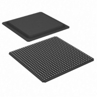
XC2V2000-4FGG676C Xilinx Inc, XC2V2000-4FGG676C Datasheet - Page 45

XC2V2000-4FGG676C
Manufacturer Part Number
XC2V2000-4FGG676C
Description
FPGA Virtex-II™ Family 2M Gates 24192 Cells 650MHz 0.15um/0.12um (CMOS) Technology 1.5V 676-Pin FBGA
Manufacturer
Xilinx Inc
Series
Virtex™-IIr
Datasheet
1.XC2V250-4FGG256C.pdf
(318 pages)
Specifications of XC2V2000-4FGG676C
Package
676FBGA
Family Name
Virtex-IIÂ
Device Logic Units
24192
Device System Gates
2000000
Number Of Registers
21504
Maximum Internal Frequency
650 MHz
Typical Operating Supply Voltage
1.5 V
Maximum Number Of User I/os
456
Ram Bits
1032192
Number Of Labs/clbs
2688
Total Ram Bits
1032192
Number Of I /o
456
Number Of Gates
2000000
Voltage - Supply
1.425 V ~ 1.575 V
Mounting Type
Surface Mount
Operating Temperature
0°C ~ 85°C
Package / Case
676-BBGA
Lead Free Status / RoHS Status
Lead free / RoHS Compliant
Number Of Logic Elements/cells
-
Lead Free Status / RoHS Status
Lead free / RoHS Compliant
Other names
122-1351
Available stocks
Company
Part Number
Manufacturer
Quantity
Price
Company:
Part Number:
XC2V2000-4FGG676C
Manufacturer:
Xilinx Inc
Quantity:
10 000
- Current page: 45 of 318
- Download datasheet (3Mb)
Virtex-II FPGA device. Timing is similar to the Slave Serial-
MAP mode except that CCLK is supplied by the Virtex-II
FPGA.
Boundary-Scan (JTAG, IEEE 1532) Mode
In Boundary-Scan mode, dedicated pins are used for con-
figuring the Virtex-II device. The configuration is done
entirely through the IEEE 1149.1 Test Access Port (TAP).
Virtex-II device configuration using Boundary-Scan is com-
patible with the IEEE 1149.1-1993 standard and the new
Table 25: Virtex-II Configuration Mode Pin Settings
Table 26
each device.
Table 26: Virtex-II Bitstream Lengths
Configuration Sequence
The configuration of Virtex-II devices is a three-phase pro-
cess after Power On Reset or POR. POR occurs when
V
DS031-2 (v3.5) November 5, 2007
Product Specification
Notes:
1. The HSWAP_EN pin controls the pull-ups. Setting M2, M1, and M0 selects the configuration mode, while the HSWAP_EN pin
2. Daisy chaining is possible only in modes where Serial D
Master Serial
Slave Serial
Master SelectMAP
Slave SelectMAP
Boundary-Scan
CCINT
controls whether or not the pull-ups are used.
support daisy chaining of downstream devices.
XC2V1000
XC2V1500
XC2V2000
XC2V3000
XC2V4000
XC2V6000
XC2V8000
XC2V250
XC2V500
XC2V40
XC2V80
Device
Configuration Mode
is greater than 1.2V, V
lists the total number of bits required to configure
R
# of Configuration Bits
(1)
CCAUX
10,494,368
15,659,936
21,849,504
26,194,208
1,593,632
2,560,544
4,082,592
5,170,208
6,812,960
338,976
598,816
is greater than 2.5V,
M2
0
1
0
1
1
M1
0
1
1
1
0
www.xilinx.com
OUT
is used. For example, in SelectMAP modes, the first device does NOT
M0
0
1
1
0
1
IEEE 1532 standard for In-System Configurable (ISC)
devices. The IEEE 1532 standard is backward compliant
with the IEEE 1149.1-1993 TAP and state machine. The
IEEE Standard 1532 for In-System Configurable (ISC)
devices is intended to be programmed, reprogrammed, or
tested on the board via a physical and logical protocol.
Configuration through the Boundary-Scan port is always
available, independent of the mode selection. Selecting the
Boundary-Scan mode simply turns off the other modes.
and V
ages have been reached, the three-phase process begins.
First, the configuration memory is cleared. Next, con-
figuration data is loaded into the memory, and finally, the
logic is activated by a start-up process.
Configuration is automatically initiated on power-up unless
it is delayed by the user. The INIT_B pin can be held Low
using an open-drain driver. An open-drain is required since
INIT_B is a bidirectional open-drain pin that is held Low by a
Virtex-II FPGA device while the configuration memory is
being cleared. Extending the time that the pin is Low causes
the configuration sequencer to wait. Thus, configuration is
delayed by preventing entry into the phase where data is
loaded.
The configuration process can also be initiated by asserting
the PROG_B pin. The end of the memory-clearing phase is
signaled by the INIT_B pin going High, and the completion
of the entire process is signaled by the DONE pin going
High. The Global Set/Reset (GSR) signal is pulsed after the
last frame of configuration data is written but before the
start-up sequence. The GSR signal resets all flip-flops on
the device.
The default start-up sequence is that one CCLK cycle after
DONE goes High, the global 3-state signal (GTS) is
released. This permits device outputs to turn on as neces-
sary. One CCLK cycle later, the Global Write Enable (GWE)
signal is released. This permits the internal storage ele-
CCLK Direction
CCO
Virtex-II Platform FPGAs: Functional Description
(bank 4) is greater than 1.5V. Once the POR volt-
Out
Out
N/A
In
In
Data Width
1
1
8
8
1
Serial D
Module 2 of 4
Yes
Yes
No
No
No
OUT
(2)
37
Related parts for XC2V2000-4FGG676C
Image
Part Number
Description
Manufacturer
Datasheet
Request
R

Part Number:
Description:
IC VIRTEX-II FPGA 2M 896-FCBGA
Manufacturer:
Xilinx Inc
Datasheet:

Part Number:
Description:
IC FPGA VIRTEX-II 2M 575-MBGA
Manufacturer:
Xilinx Inc
Datasheet:

Part Number:
Description:
IC FPGA VIRTEX-II 2M 676-FBGA
Manufacturer:
Xilinx Inc
Datasheet:

Part Number:
Description:
IC FPGA VIRTEX-II 2M 676-FBGA
Manufacturer:
Xilinx Inc
Datasheet:

Part Number:
Description:
IC FPGA VIRTEX-II 2M 575-MBGA
Manufacturer:
Xilinx Inc
Datasheet:

Part Number:
Description:
IC FPGA VIRTEX-II 2M 575-MBGA
Manufacturer:
Xilinx Inc
Datasheet:

Part Number:
Description:
IC FPGA VIRTEX-II 2M 896-FBGA
Manufacturer:
Xilinx Inc
Datasheet:

Part Number:
Description:
IC FPGA VIRTEX-II 2M 896-FBGA
Manufacturer:
Xilinx Inc
Datasheet:

Part Number:
Description:
IC FPGA VIRTEX-II 2M 676-FBGA
Manufacturer:
Xilinx Inc
Datasheet:

Part Number:
Description:
IC FPGA VIRTEX-II 2M 676-FBGA
Manufacturer:
Xilinx Inc
Datasheet:

Part Number:
Description:
IC FPGA VIRTEX-II 2M 575-MBGA
Manufacturer:
Xilinx Inc
Datasheet:

Part Number:
Description:
IC FPGA VIRTEX-II 2M 575-MBGA
Manufacturer:
Xilinx Inc
Datasheet:

Part Number:
Description:
IC FPGA VIRTEX-II 2M 896-FBGA
Manufacturer:
Xilinx Inc
Datasheet:

Part Number:
Description:
IC FPGA VIRTEX-II 575PBGA
Manufacturer:
Xilinx Inc
Datasheet:

Part Number:
Description:
IC FPGA VIRTEX-II 896FCBGA
Manufacturer:
Xilinx Inc
Datasheet:


