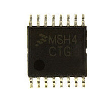
MC9S08SH4CTG Freescale, MC9S08SH4CTG Datasheet - Page 47

MC9S08SH4CTG
Manufacturer Part Number
MC9S08SH4CTG
Description
Manufacturer
Freescale
Datasheet
1.MC9S08SH4CTG.pdf
(338 pages)
Specifications of MC9S08SH4CTG
Cpu Family
HCS08
Device Core Size
8b
Frequency (max)
40MHz
Interface Type
I2C/SCI/SPI
Total Internal Ram Size
256Byte
# I/os (max)
13
Number Of Timers - General Purpose
1
Operating Supply Voltage (typ)
3.3/5V
Operating Supply Voltage (max)
5.5V
Operating Supply Voltage (min)
2.7V
On-chip Adc
8-chx10-bit
Instruction Set Architecture
CISC
Operating Temp Range
-40C to 85C
Operating Temperature Classification
Industrial
Mounting
Surface Mount
Pin Count
16
Package Type
TSSOP
Program Memory Type
Flash
Program Memory Size
4KB
Lead Free Status / RoHS Status
Compliant
Available stocks
Company
Part Number
Manufacturer
Quantity
Price
Company:
Part Number:
MC9S08SH4CTG
Manufacturer:
FREESCAL
Quantity:
96
Company:
Part Number:
MC9S08SH4CTG
Manufacturer:
Freescale
Quantity:
8 727
- Current page: 47 of 338
- Download datasheet (4Mb)
4.5.1
Features of the FLASH memory include:
4.5.2
Before any program or erase command can be accepted, the FLASH clock divider register (FCDIV) must
be written to set the internal clock for the FLASH module to a frequency (f
200 kHz (see
once, so normally this write is done during reset initialization. FCDIV cannot be written if the access error
flag, FACCERR in FSTAT, is set. The user must ensure that FACCERR is not set before writing to the
FCDIV register. One period of the resulting clock (1/f
program and erase pulses. An integer number of these timing pulses are used by the command processor
to complete a program or erase command.
Table 4-5
of FCLK (f
of cycles of FCLK and as an absolute time for the case where t
shown include overhead for the command state machine and enabling and disabling of program and erase
voltages.
Freescale Semiconductor
•
•
•
•
•
•
•
FLASH size
— MC9S08SH8: 8,192 bytes (16 pages of 512 bytes each)
— MC9S08SH4: 4,096 bytes (8 pages of 512 bytes each)
Single power supply program and erase
Command interface for fast program and erase operation
Up to 100,000 program/erase cycles at typical voltage and temperature
Flexible block protection
Security feature for FLASH and RAM
Auto power-down for low-frequency read accesses
shows program and erase times. The bus clock frequency and FCDIV determine the frequency
Program and Erase Times
FCLK
Features
Section 4.7.1, “FLASH Clock Divider Register
Byte program
Byte program (burst)
Page erase
Mass erase
1
). The time for one cycle of FCLK is t
Excluding start/end overhead
Parameter
MC9S08SH8 MCU Series Data Sheet, Rev. 3
Table 4-5. Program and Erase Times
Cycles of FCLK
20,000
4000
9
4
FCLK
FCLK
) is used by the command processor to time
= 1/f
(FCDIV)”). This register can be written only
FCLK
FCLK
Time if FCLK = 200 kHz
= 5 μs. Program and erase times
. The times are shown as a number
FCLK
100 ms
20 μs
20 ms
45 μs
) between 150 kHz and
1
Chapter 4 Memory
47
Related parts for MC9S08SH4CTG
Image
Part Number
Description
Manufacturer
Datasheet
Request
R

Part Number:
Description:
TOWER ELEVATOR BOARDS HARDWARE
Manufacturer:
Freescale Semiconductor
Datasheet:

Part Number:
Description:
TOWER SERIAL I/O HARDWARE
Manufacturer:
Freescale Semiconductor
Datasheet:

Part Number:
Description:
LCD MODULE FOR TWR SYSTEM
Manufacturer:
Freescale Semiconductor
Datasheet:

Part Number:
Description:
DAUGHTER LCD WVGA I.MX51
Manufacturer:
Freescale Semiconductor
Datasheet:

Part Number:
Description:
TOWER SYSTEM BOARD MPC5125
Manufacturer:
Freescale Semiconductor
Datasheet:

Part Number:
Description:
KIT EVALUATION I.MX51
Manufacturer:
Freescale Semiconductor
Datasheet:

Part Number:
Description:
KIT DEVELOPMENT WINCE IMX25
Manufacturer:
Freescale Semiconductor
Datasheet:

Part Number:
Description:
TOWER SYSTEM KIT MPC5125
Manufacturer:
Freescale Semiconductor
Datasheet:

Part Number:
Description:
TOWER SYSTEM BOARD K40X256
Manufacturer:
Freescale Semiconductor
Datasheet:

Part Number:
Description:
TOWER SYSTEM KIT K40X256
Manufacturer:
Freescale Semiconductor
Datasheet:

Part Number:
Description:
Microcontrollers (MCU) MX28 PLATFORM DEV KIT
Manufacturer:
Freescale Semiconductor
Datasheet:

Part Number:
Description:
MCU, MPU & DSP Development Tools IAR KickStart Kit for Kinetis K60
Manufacturer:
Freescale Semiconductor
Datasheet:

Part Number:
Description:
24BIT HDMI MX535/08
Manufacturer:
Freescale Semiconductor
Datasheet:
Part Number:
Description:
Manufacturer:
Freescale Semiconductor, Inc
Datasheet:
Part Number:
Description:
Manufacturer:
Freescale Semiconductor, Inc
Datasheet:


